© 2004 National Semiconductor Corporation
General Description
The CLC730231 evaluation board is designed to aid in the
characterization of National Semiconductor’s High Speed
quad SOIC operational amplifiers.
Use the evaluation board as a guide for high frequency
layout and as a tool to aid in device testing and character-
ization.
The evaluation board schematic is shown below in Figure 1.
Refer to the product data sheets for recommendations for
component values.
Basic Operation
By changing RIN and ROUT different input and output im-
pedances can be matched. The SMA connectors and board
traces are optimized for 50 to 75Ω operation. Other imped-
ances can be matched but performance may be noticeably
different, especially high frequency response. Even with op-
timal layout board parasitics play a large part in high fre-
quency performance and different termination resistors will
change the frequency of the dominant parasitic poles/zeros.
Layout Considerations
Printed circuit board layout and supply bypassing play major
roles in determining high frequency performance. When de-
signing your own board use these evaluation boards as a
guide and follow these steps to optimize high frequency
performance:
1. Use a ground plane
2. Include large ( ~ 6.8 µF) capacitors on both supplies.
3. Near the device use .01 µF ceramic capacitors from both
4. Remove the ground and power planes from under and
5. Minimize all trace lengths
CLC730231 Quad High Speed SOIC Op Amp Evaluation
supplies to ground C1, C2.
around the part, especially the input and output pins.
MS200972
Board
6. Use terminated transmission lines for long traces.
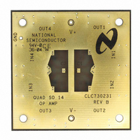
Sample artwork for the CLC730231 Evaluation board is
included on the next page in Figure 2.
Inverting Operation
With slight modification this board can be modified for invert-
ing operation. Cut the input trace between the SMA connec-
tor and the RIN resistor leaving RIN connected to the non
inverting pin ( the non-inverting input needs a DC bias cur-
rent path). Solder a resistor between the input line and the
inverting input side of R
Leave R
as marked. For matching input impedance a parallel termi-
nating resistor can be added from the input line to the
unused ground pad from the empty R
sary trace cuts are shown in Figure 4.
Measurement Hints
The board is designed for 50Ω input and output connections
into coaxial cables. For other impedances the terminating
resistors can be modified to help match different imped-
ances.
Do not use normal oscilloscope probes to test these circuits.
The capacitive loading will change circuit performance dras-
tically. Instead use low impedance resistive divider probes of
100 to 500Ω. See Figure 3 for a sample resistive probe. The
Low impedance resistor should be 50- 450Ω. The ground
connection should be as short as possible ( ~ 1/2”). Even with
careful use of these probes results should be considered
preliminary until verified with controlled impedance measure-
ments. Even the best probes will interfere with circuit opera-
tion to some degree. Also, tools, power cables, fingers etc.
near the device will change measurement results often
dramatically.
G
empty and all other components should be loaded
F
(the side closest to the input trace).
G
space. The neces-
www.national.com
March 2004