AD8332-EVALZ Analog Devices Inc, AD8332-EVALZ Datasheet
AD8332-EVALZ
Specifications of AD8332-EVALZ


Related parts for AD8332-EVALZ


AD8332-EVALZ Summary of contents
Page 1
... ADC. An external resistor adjusts the clamping level. The operating temperature range is −40°C to +85°C. The AD8331 is available in a 20-lead QSOP package, the AD8332 is available in 28-lead TSSOP and 32-lead LFCSP packages, and the AD8334 is available in a 64-lead LFCSP package. ...
Page 2
... Changes to Figure 104 ................................................................... 43 Changes to Figure 106 ................................................................... 45 Changes to Figure 107 ................................................................... 46 Changes to Figure 113 ................................................................... 47 Changes to Figure 114 and Board Layout Section ..................... 48 Deleted AD8332 Bill of Materials Section and Table 13; Renumbered Sequentially ............................................................. 48 Changes to Figure 115 ................................................................... 49 Changes to Figure 116 ................................................................... 50 Changes to Figure 117 to Figure 120 ........................................... 51 Changes to Figure 121 ................................................................... 52 Deleted AD8334 Bill of Materials Section and Table 15 ...
Page 3
... Changes to User-Supplied Optional Components Section and Measurement Setup Section ................................................... 39 Changes to Figure 95 ...................................................................... 39 Changes to Figure 97 ...................................................................... 41 Added Figure 98 .............................................................................. 42 Incorporated AD8332-EVALZ Data Sheet, Rev. D ..................... 44 Incorporated AD8334-EVAL Data Sheet, Rev. 0 ........................ 49 Updated Outline Dimensions ........................................................ 55 Changes to Ordering Guide ........................................................... 57 4/06—Rev Rev. E Added AD8334 ................................................................... Universal Changes to Figure 1 and Figure 2 ...
Page 4
... Large Signal Bandwidth AD8331 AD8332, AD8334 Slew Rate AD8331 AD8332, AD8334 Input Voltage Noise Noise Figure Active Termination Match Unterminated Output-Referred Noise AD8331 AD8332, AD8334 Output Impedance, Postamplifier = 50 Ω 280 Ω pF MHz Test Conditions/Comments Single-ended input to differential output Input to output (single-ended) AC-coupled R = 280 Ω ...
Page 5
... HD2 HD3 Input 1 dB Compression Point Two-Tone Intermodulation Distortion (IMD3) AD8331 AD8332, AD8334 Output Third-Order Intercept AD8331 AD8332, AD8334 Channel-to-Channel Crosstalk (AD8332, AD8334) Overload Recovery Group Delay Variation ACCURACY 2 Absolute Gain Error Gain Law Conformance 3 Channel-to-Channel Gain Matching GAIN CONTROL INTERFACE (Pin GAIN) ...
Page 6
... Power-Down Current AD8331 AD8332 AD8334 LNA Current AD8331 (ENBL) AD8332, AD8334 (ENBL) VGA Current AD8331 (ENBV) AD8332, AD8334 (ENBV) PSRR 1 All dBm values are referred to 50 Ω. 2 The absolute gain refers to the theoretical gain expression in Equation 1. 3 Best-fit to linear-in-dB curve. 4 The current is limited to ±1 mA typical. ...
Page 7
... Voltage Supply Voltage (VPSn, VPSV, VPSL, VPOS) Input Voltage (INHx) ENB, ENBL, ENBV, HILO Voltage GAIN Voltage Power Dissipation 1 RU Package (AD8332) CP-32 Package (AD8332 Package (AD8331) CP-64 Package (AD8334) Temperature Operating Temperature Range Storage Temperature Range Lead Temperature (Soldering 60 sec) θ ...
Page 8
... AD8331/AD8332/AD8334 PIN CONFIGURATIONS AND FUNCTION DESCRIPTIONS Table 3. 20-Lead QSOP Pin Function Description (AD8331) Pin No. Mnemonic 1 LMD 2 INH 3 VPSL 4 LON 5 LOP 6 COML 7 VIP 8 VIN 9 MODE 10 GAIN 11 VCM 12 RCLMP 13 HILO 14 VPOS 15 VOH 16 VOL 17 COMM 18 ENBV 19 ENBL 20 COMM LMD COMM 1 20 PIN 1 ENBL INH ...
Page 9
... VOH2 12 17 VOL2 13 16 COMM 14 15 Figure 4. 28-Lead TSSOP Pin Configuration (AD8332) Table 4. 28-Lead TSSOP Pin Function Description (AD8332) Pin No. Mnemonic Description 1 LMD2 CH 2 LNA Midsupply Pin; Connect a Capacitor for Midsupply HF Bypass 2 INH2 CH2 LNA Input 3 VPS2 CH2 Supply LNA 5 V ...
Page 10
... AD8331/AD8332/AD8334 Table 6. 64-Lead LFCSP Pin Function Description (AD8334) Pin No. Mnemonic 1 INH2 2 LMD2 LON2 5 LOP2 6 VIP2 7 VIN2 8 VPS2 9 VPS3 10 VIN3 11 VIP3 12 LOP3 13 LON3 LMD3 16 INH3 17 COM3 18 COM4 19 INH4 20 LMD4 LON4 23 LOP4 24 VIP4 25 VIN4 26 VPS4 INH2 1 PIN 1 INDICATOR LMD2 LON2 4 LOP2 5 VIP2 6 VIN2 ...
Page 11
... CH1 LNA Feedback Output (for Not Connected LNA Midsupply Pin; Connect a Capacitor for Midsupply HF Bypass. CH1 LNA Input. CH1 LNA Ground. CH2 LNA Ground. The exposed paddle must be soldered to the PCB ground to ensure proper heat dissipation, noise, and mechanical strength benefits. Rev Page AD8331/AD8332/AD8334 ...
Page 12
... AD8331/AD8332/AD8334 TYPICAL PERFORMANCE CHARACTERISTICS T = 25° 500 Ω −4 +43.5 dB gain (HILO = LO), and differential output voltage, unless otherwise specified HILO = HILO = LO 0 ASCENDING GAIN MODE DESCENDING GAIN MODE (WHERE AVAILABLE) –10 0 0.2 0.4 0.6 V (V) GAIN Figure 7. Gain vs. V and MODE (MODE Available on RU Package) GAIN 2 ...
Page 13
... Figure 17. Group Delay vs. Frequency for Two Values of AC Coupling 100M 500M Figure 18. Representative Differential Output Offset Voltage vs Ω S Rev Page AD8331/AD8332/AD8334 p-p OUT – 1.0V GAIN AD8332 V = 0.7V –40 GAIN AD8334 V = 0.4V GAIN –60 –80 100k 1M 10M FREQUENCY (Hz) Figure 16. Channel-to-Channel Crosstalk vs. ...
Page 14
... AD8331/AD8332/AD8334 35 SAMPLE SIZE = 100 0.2V < V < 0.7V GAIN 49.6 49.7 49.8 49.9 50.0 50.1 GAIN SCALING FACTOR Figure 19. Gain Scaling Factor Histogram 100 SINGLE ENDED, PIN VOH OR PIN VOL ∞ 0.1 100k 1M FREQUENCY (Hz) Figure 20. Output Impedance vs. Frequency 10k 1k 100 R = ∞ 0pF R = 549Ω ...
Page 15
... Figure 28. Short-Circuit, Input-Referred Noise vs. Temperature GAIN 5MHz 0.1 100M 1 7 INCLUDES NOISE OF VGA SIMULATED RESULTS 0 0.8 1.0 50 Figure 30. Noise Figure vs. R GAIN Rev Page AD8331/AD8332/AD8334 ∞ 1V 10MHz GAIN –30 – TEMPERATURE (°C) ∞ GAIN R THERMAL NOISE S ALONE 10 100 SOURCE RESISTANCE (Ω ...
Page 16
... AD8331/AD8332/AD8334 35 PREAMP LIMITED HILO = LO 50Ω IN ∞ HILO = LO HILO = HI 50Ω IN ∞ HILO = HI 0.1 0.2 0.3 0.4 0.5 0.6 V (V) GAIN Figure 31. Noise Figure vs 10MHz 50Ω GAIN (dB) Figure 32. Noise Figure vs. Gain 30dB V = 1Vp-p OUT –10 –20 –30 –40 –50 –60 –70 – ...
Page 17
... Figure 41. Output Third-Order Intercept (IP3) vs. V 2mV 100 50mV 0.8 0.9 1.0 Figure 42. Small Signal Pulse Response dB, Top: Input, Bottom: Output Voltage, HILO = Rev Page AD8331/AD8332/AD8334 p-p COMPOSITE ( + ) OUT 1 2 HILO = LO HILO = HI 10M FREQUENCY (Hz) Figure 40. IMD3 vs. Frequency 1MHz HILO = LO 10MHz HILO = LO ...
Page 18
... AD8331/AD8332/AD8334 20mV 100 500mV Figure 43. Large Signal Pulse Response dB, HILO = HI or LO, Top: Input, Bottom: Output Voltage 30dB 1 INPUT 0 –1 INPUT IS NOT TO SCALE –2 –50 –40 –30 –20 – TIME (ns) Figure 44. Large Signal Pulse Response for Various Capacitive Loads pF, 10 pF 500mV 200mV Figure 45 ...
Page 19
... Figure 52. Enable Response, Large Signal, Top Bottom 150 mV p-p ENB OUT INH 0 VPS1, V GAIN VPSV 0.5V GAIN VPS1, V GAIN 100k 1M 10M FREQUENCY (Hz) Figure 53. PSRR vs. Frequency (No Bypass Capacitor 0.5V GAIN AD8334 AD8332 AD8331 –40 – TEMPERATURE (°C) Figure 54. Quiescent Supply Current vs. Temperature = 0. 100M 80 100 ...
Page 20
... AD8331/AD8332/AD8334 TEST CIRCUITS MEASUREMENT CONSIDERATIONS Figure 55 through Figure 68 show typical measurement configurations and proper interface values for measurements with 50 Ω conditions. Short-circuit input noise measurements are made as shown in Figure 62. The input-referred noise level is determined by Figure 56. Test Circuit—Frequency Response for Various Matched Source Impedances Figure 57. Test Circuit— ...
Page 21
... Figure 60. Test Circuit—Frequency Response for Unterminated LNA, Single-Ended 18nF 270Ω FB* 120nH 0.1µF INH DUT 22pF 0.1µF LMD *FERRITE BEAD Figure 61. Test Circuit—Short-Circuit, Input-Referred Noise Rev Page AD8331/AD8332/AD8334 50Ω IN 0.1µF OR 0.1µF 1µF 237Ω 28Ω VGA 1:1 237Ω LMD 0.1µF 0.1µ ...
Page 22
... INH DUT 1kΩ 22pF LMD 28Ω 0.1µF 0.1µF Figure 63. Test Circuit—Harmonic Distortion vs. Load Resistance 18nF 270Ω AD8332 0.1µF 237Ω 0.1µF 28Ω INH DUT 237Ω 22pF LMD 0.1µF 28Ω 0.1µF Figure 64. Test Circuit— ...
Page 23
... FB* 0.1µF 120nH INH DUT 22pF 50Ω LMD RF 0.1µF SIGNAL 0.1µF GENERATOR *FERRITE BEAD Figure 68. Test Circuit—PSRR vs. Frequency Rev Page AD8331/AD8332/AD8334 OSCILLOSCOPE 50Ω IN 28Ω 1:1 28Ω OSCILLOSCOPE CH1 CH2 DIFF PROBE 9.5dB 50Ω PULSE GENERATOR NETWORK ANALYZER 50Ω ...
Page 24
... LMD1 VGA BIAS AND LNA V MID INTERPOLATOR LMD2 + ATTENUATOR INH2 LNA 2 –48dB – AD8332 LON2 LOP2 VIP2 VIN2 ENB Figure 70. AD8332 Functional Block Diagram INH1 LMD1 LMD2 HILO 3.5dB/ INH2 15.5dB VOH LON2 21dB PA LOP2 VOL VIP2 VIN2 MODE GAIN INT ...
Page 25
... Low HD2 is particularly important in second harmonic ultrasound imaging applications. Differential signaling enables smaller swings at each output, further reducing third-order distortion. Rev Page AD8331/AD8332/AD8334 AD8331/AD8332/AD8334 (can be the same value as LMD ) is connected from the LMD INH C R ...
Page 26
... AD8331/AD8332/AD8334 Active Impedance Matching The LNA supports active impedance matching through an external shunt feedback resistor from Pin LON to Pin INH. The input resistance given in Equation 5, where A is the single- IN ended gain of 4.5, and 6 kΩ is the unterminated input impedance. × kΩ ...
Page 27
... When V gain errors are slightly greater. The gain slope can be inverted, as shown in Figure 73 (except for the AD8332 AR models). The gain drops with a slope of −50 dB/V – across the gain control range from maximum to minimum gain. POSTAMP ...
Page 28
... AD8331/AD8332/AD8334 VGA Noise In a typical application, a VGA compresses a wide dynamic range input signal to within the input span of an ADC. While the input-referred noise of the LNA limits the minimum resolvable input signal, the output-referred noise, which depends primarily on the VGA, limits the maximum instantaneous dynamic range that can be processed at any one particular gain control voltage ...
Page 29
... For additional information, see the Applications Information section. The accuracy of the clamping levels is approximately ± mode. Figure 80 illustrates the output characteristics for a few values CLMP AD8331/AD8332/AD8334 5.0 4.5 ∞ CLMP 4.0 8.8kΩ ...
Page 30
... RCLMP ENB * 12 17 VOH2 VGA OUT VOH1 * 13 16 VOL2 VGA OUT VOL1 14 15 COMM VPSV 5V 1nF 0.1µF *SEE TEXT (AD8332 LNA DECOUPLING R RESISTOR IZ VIP 5Ω 50Ω LON 3.25V VCM 2.5V LNA 2.5V LOP 5Ω 50Ω 3.25V VIN LNA DECOUPLING RESISTOR ...
Page 31
... Gain Input The GAIN pin is common to both channels of the AD8332. The input impedance is nominally 10 MΩ, and a bypass capacitor from 100 recommended. Parallel connected devices can be driven by a common voltage source or DAC. Decoupling should take into account any band- width considerations of the drive waveform, using the total distributed capacitance ...
Page 32
... AD8331/AD8332/AD8334 with gains less than 40 dB. The exact values of these components can be selected empirically. An antialiasing noise filter is typically used with an ADC. Filter requirements are application dependent. When the ADC resides on a separate board, the majority of filter components should be placed nearby to suppress noise picked up between boards and to mitigate charge kickback from the ADC inputs ...
Page 33
... ADG736 dual SPDT Analog Devices Rev Page AD8331/AD8332/AD8334 ADG736 1.13kΩ SELECT R IZ 280Ω 18nF 5Ω 200Ω INH LNA LMD 50Ω 0.1µF AD8332 Figure 89. Accommodating Multiple Sources AD8331 as an example COMM LMD AD8331 INH ENBL + VPSL ...
Page 34
... Figure 91 through Figure 93 are schematics of a dual, fully differential system using the AD8332 and the high speed ADC with conversion speeds as high as 65 MSPS. HIGH DENSITY QUAD LAYOUT ...
Page 35
... L11 VOL2 VOL1 120nH L10 COMM VPSV 120nH FB R26 100Ω +5VGA C45 C85 0.1µF 1nF AD8332 Rev Page AD8331/AD8332/AD8334 TP6 L13 C60 120nH FB 0.1µ C79 IN1 22pF CFB1 18nF RFB1 274Ω C42 C59 0.1µF 0.1µF ...
Page 36
... JP1 D3_B D4_B U5 74VHC04 13 12 D5_B 11 10 +3.3VADDIG U5 C26 74VHC04 0.1µF Figure 92. Converter Schematic, TGC Using an AD8332 Rev Page C22 C21 0.1µF 1nF ADCLK R11 100Ω R10 1 64 JP2 AGND AVDD 0Ω SHARED REF 2 63 VIN+_A CLK_A Y ...
Page 37
... C8 C10 C76 0.1µF 0.1µF 10µF 6. +3.3VDVDD + + C27 C7 C9 10µF 0.1µF 0.1µF 6. C75 10µF 0.1µF 0.1µF 0.1µF 6. AD8332 and AD9238 Rev Page AD8331/AD8332/AD8334 R40 22Ω × × 4 RP2 × × SAM080UPM ...
Page 38
... AD8331/AD8332/AD8334 COM3 COM4 INH4 LMD4 NC LON4 LOP4 VIP4 VIN4 VPS4 GAIN34 CLMP34 HILO VCM4 VCM3 NC 03199-094 Figure 94. Compact Signal Path and Board Layout for the Rev Page COM2 COM1 INH1 LMD1 NC LON1 LOP1 VIP1 VIN1 VPS1 GAIN12 CLMP12 EN12 EN34 VCM1 ...
Page 39
... Left = high gain Right = LO gain BOARD LAYOUT The evaluation board circuitry uses four conductor layers. The two inner layers are grounded, and all interconnecting circuitry is located on the outer layers. Figure 99 to Figure 102 illustrate the copper patterns. Rev Page AD8331/AD8332/AD8334 GAIN GAIN ...
Page 40
... AD8331/AD8332/AD8334 AD8331 EVALUATION BOARD SCHEMATICS GND1 GND2 GND +5V C INH L1 0.1µF LNA2 120nH FB PROBE 3 D1 INPUT CLAMP BAT64-04 120nH FB DIODES +5V LON R4 R8 LOP GN_SLOPE COMPONENTS IN GRAY ARE OPTIONAL AND USER SUPPLIED LMD2 COMM 10µF CLMD 10V 0.1µF 2 INH ENB ...
Page 41
... ANALYZER DP8200 PRECISION VOLTAGE REFERENCE (FOR VGAIN) Figure 97 1103 TEKPROBE POWER SUPPLY +5V GND DIFFERENTIAL PROBE TO VO PINS INSERT JUMPERS W5 AND W6 TO USE OUTPUT TRANSFORMER AND VOH SMA AD8331 Typical Board Test Connections Rev Page AD8331/AD8332/AD8334 E3631A POWER SUPPLY ...
Page 42
... AD8331/AD8332/AD8334 AD8331 EVALUATION BOARD PCB LAYERS Figure 98. AD8331-EVALZ Assembly Figure 99. Primary Side Copper Figure 100. Secondary Side Copper Figure 101. Internal Layer Ground Figure 102. Power Plane Figure 103. Top Silkscreen Rev Page ...
Page 43
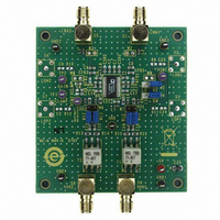
... AD8332 EVALUATION BOARD GENERAL DESCRIPTION The AD8332-EVALZ is a platform for the testing and evaluation of the AD8332 variable gain amplifier (VGA). The board is shipped assembled and tested, and users need only connect the signal and VGAIN sources to a single 5 V power supply. Figure 104 is a photograph of the component side of the board, and Figure 105 shows the schematic ...
Page 44
... VOH2 VOH1 R7 100Ω VOL2 VOL1 R8 100Ω 120nH FB 120nH FB COMM VPSV C22 0.1µF Figure 105. Schematic of the AD8332 Evaluation Board Rev Page 0.1µF C3 CSH1 L2 0.1µF LNA1 22pF 120nH FB CFB1 CAL1 18nF +5VLNA C7 0.1µF S2 LON1 C23 R9 ...
Page 45
... VGAIN SUPPLY Figure 106. NETWORK ANALYZER AD8332 Typical Board Test Connections Rev Page AD8331/AD8332/AD8334 1103 TEKPROBE POWER SUPPLY DIFFERENTIAL PROBE ...
Page 46
... AD8331/AD8332/AD8334 AD8332 EVALUATION BOARD PCB LAYERS Figure 107. AD8332-EVALZ Assembly Figure 108. Primary Side Copper Figure 109. Secondary Side Copper Figure 110. Ground Plane Figure 111. Power Plane Figure 112. Component Side Silkscreen Rev Page ...
Page 47
... The board is shipped assembled and tested, and users need only connect the signal and VGAIN sources and a single 5 V power supply. Figure 113 is a photograph of the board. The AD8334-EVALZ is lead free and RoHS compliant. Figure 113. AD8334-EVALZ Top View Rev Page AD8331/AD8332/AD8334 ...
Page 48
... AD8331/AD8332/AD8334 CONFIGURING THE INPUT IMPEDANCE The board is built and tested using the components shown in black in Figure 115. Provisions are made for optional components (shown in gray) that can be installed at user discretion. As shipped, the input impedances of the low noise amplifiers (LNAs) are configured for 50 Ω to match the output impedances of most signal generators and network analyzers. Input impedances kΩ ...
Page 49
... C32 I N4 0.1 µF L4 ICR4 120 R22 R23 120 +5V 1 LO4 3 CR4 Figure 115. AD8334-EVALZ Schematic Rev Page AD8331/AD8332/AD8334 +5V +5V R49 120 nH 4.02kΩ RX1 100Ω EN34 E E 100Ω C57 D D 0.1 µF C59 120 nH 0.1 µ ...
Page 50
... AD8331/AD8332/AD8334 PRECISION VOLTAGE REFERENCE (FOR VGAIN) NETWORK ANALYZER SIGNAL INPUT Figure 116. GAIN CONTROL VOLTAGE GND AD8334 Typical Board Test Connections (One Channel Shown) Rev Page PROBE POWER SUPPLY +5V DIFFERENTIAL PROBE POWER SUPPLY GND ...
Page 51
... AD8334 EVALUATION BOARD PCB LAYERS Figure 117. AD8334-EVALZ Primary Side Copper Figure 118. AD8334-EVALZ Secondary Side Copper AD8331/AD8332/AD8334 Figure 119. AD8334-EVALZ Inner Layer 1Copper Figure 120. AD8334-EVALZ Inner Layer 2 Copper Rev Page ...
Page 52
... AD8331/AD8332/AD8334 Figure 121. AD8334-EVALZ Component Side Silkscreen Rev Page ...
Page 53
... SEATING PLANE 0.012 (0.30) BSC 0.008 (0.20) COMPLIANT TO JEDEC STANDARDS MO-137-AD Figure 123. 20-Lead Shrink Small Outline Package (QSOP) (RQ-20) Dimensions shown in Inches and (millimeters Rev Page AD8331/AD8332/AD8334 6.40 BSC 8 ° 0.75 0 ° 0.60 0.45 0.010 (0.25) 0.020 (0.51) 0.006 (0.15) ...
Page 54
... AD8331/AD8332/AD8334 PIN 1 INDICATOR 12° MAX 1.00 0.85 0.80 SEATING PLANE BSC SQ PIN 1 INDICATOR 1.00 12° MAX 0.85 0.80 SEATING PLANE 5.00 BSC SQ 0.60 MAX 24 0.50 BSC TOP 4.75 VIEW BSC SQ 0.50 0.40 17 0.30 0.80 MAX 0.65 TYP 0.05 MAX 0.02 NOM ...
Page 55
... AD8332ARU-REEL7 –40°C to +85°C AD8332ARUZ –40°C to +85°C AD8332ARUZ-R7 –40°C to +85°C AD8332ARUZ-RL –40°C to +85°C AD8332-EVALZ AD8334ACPZ –40°C to +85°C AD8334ACPZ-REEL –40°C to +85°C AD8334ACPZ-REEL7 –40°C to +85°C AD8334-EVALZ RoHS Compliant Part ...
Page 56
... AD8331/AD8332/AD8334 NOTES ©2003–2010 Analog Devices, Inc. All rights reserved. Trademarks and registered trademarks are the property of their respective owners. D03199-0-10/10(G) Rev Page ...