LP38511MR-ADJEV/NOPB National Semiconductor, LP38511MR-ADJEV/NOPB Datasheet

BOARD EVALUATION FOR LP38511

LP38511MR-ADJEV/NOPB

Manufacturer Part Number
LP38511MR-ADJEV/NOPB
Description
BOARD EVALUATION FOR LP38511
Manufacturer
National Semiconductor

Specifications of LP38511MR-ADJEV/NOPB

Channels Per Ic
1 - Single
Voltage - Output
1.2V
Current - Output
800mA
Voltage - Input
2.25 ~ 5.5V
Regulator Type
Positive Adjustable
Operating Temperature
-40°C ~ 125°C
Board Type
Fully Populated
Utilized Ic / Part
LP38511
Silicon Manufacturer
National
Silicon Core Number
LP38511MR-ADJ
Kit Application Type
Power Management - Voltage Regulator
Application Sub Type
LDO
Kit Contents
Board, Doc
Lead Free Status / RoHS Status
Contains lead / RoHS non-compliant
Other names
LP38511MR-ADJEV
© 2009 National Semiconductor Corporation
LP38511MR-ADJ Evaluation
Board
Introduction
This board is designed to allow the evaluation of the
LP38511MR-ADJ Voltage Regulator. Each board is assem-
bled and tested in the factory. This evaluation board has the
PSOP-8 package mounted, and the output voltage is set to
1.20V.
General Description
The LP38511MR-ADJ is an adjustable LDO linear regulator
capable of supplying up to 800 mA of output current, and in-
corporates an Enable function.
The device has been designed to work with 10 µF input and
output ceramic capacitors. Footprints areas for C
C
Operation
The input voltage, applied between V
at least 2.25V, or at least 500 mV greater than V
er value is larger. The input voltage should be no greater than
5.5V, which is the high end of the Operating Rating voltage.
Loads can be connected to V
V
accurate measurements directly onto the input and output
pins of the device, eliminating any voltage drop on the PCB
traces or connecting wires to the load.
Setting V
The output voltage is set using the external resistive divider
R1 and R2. The output voltage is given by the formula:
It is recommended that the values selected for R1 and R2 are
such that the parallel value is less than 1.00 kΩ. This is to
prevent internal parasitic capacitances on the ADJ pin from
interfering with the F
Table 1 lists some suggested, best fit, standard ±1% resistor
values for R1 and R2, and a standard ±10% capacitor values
for C
and C
OUT
OUT
FF
will allow for a variety of sizes.
and V
FF
, for a range of V
are available that will give similar results.
IN
V
( (R1 x R2) / (R1 + R2) )
test points are provided on the board to allow
OUT
OUT
= V
Z
ADJ
pole set by R1 and C
OUT
x (1 + (R1 / R2))
values. Other values of R1, R2,
OUT
with reference to GND.
IN
and GND, should be
1.00 kΩ
300478
FF
.
OUT
, whichev-
IN
and
(1)
National Semiconductor
Application Note 1770
Don Jones
April 10, 2009
Refer to Application Note AN-1378 for additional information
on how resistor tolerances affect the calculated V
The LP38511MR-ADJ Evaluation board is assembled with a
1.40 kΩ ±1% resistor for R1, and a 1.00 kΩ ±1% resistor for
R2. This sets V
Selecting C
A capacitor placed across the gain resistor R1 will provide
additional phase margin to improve load transient response
of the device. This capacitor, C
a zero in the loop response given by the formula:
The value for C
(F
The closest standard 10% value is usually adequate for C
The LP38511MR-ADJ Evaluation board is assembled with a
3300 pF capacitor for C
kHz.
0.80V
1.00V
1.20V
1.50V
1.80V
2.00V
2.50V
3.00V
3.30V
Z
V
F
) between 25 kHz and 50 kHz using the formula:
Z
OUT
= (1 / (2 x
V
OUT
= 500 mV x (1 + (1.40 kΩ / 1.00 kΩ ) )
1.07 kΩ
1.00 kΩ
1.40 kΩ
2.00 kΩ
2.94 kΩ
1.02 kΩ
1.02 kΩ
1.00 kΩ
2.00 kΩ
F
C
R1
Z
OUT
FF
FF
π
= (1 / (2 x
should be selected to set a zero frequency
x 3300 pF x 1.40kΩ ) ) = 34.4 kHz
= 1 / (2 x
to 1.20V.
FF
1.78 kΩ
1.00 kΩ
1.00 kΩ
1.00 kΩ
1.13 kΩ
FF
TABLE 1.
340Ω
255Ω
200Ω
357Ω
. This sets F
π
R2
π
x C
x F
FF
FF
, in parallel with R1, will form
Z
x R1) )
x R1)
4700 pF
4700 pF
3300 pF
2700 pF
1500 pF
4700 pF
4700 pF
4700 pF
2700 pF
C
Z
FF
to approximately 34
www.national.com
31.6 kHz
33.8 kHz
34.4 kHz
29.5 kHz
36.1 kHz
33.2 kHz
33.2 kHz
33.8 kHz
29.5 kHz
OUT
F
value.
Z
(2)
(3)
(4)
(5)
FF
.

Related parts for LP38511MR-ADJEV/NOPB

LP38511MR-ADJEV/NOPB Summary of contents

Page 1

... This capacitor zero in the loop response given by the formula: (1) The value for between 25 kHz and 50 kHz using the formula ≤ The closest standard 10% value is usually adequate for C 1.00 kΩ The LP38511MR-ADJ Evaluation board is assembled with a 3300 pF capacitor for C kHz 300478 TABLE 4700 pF 1.07 kΩ ...

Page 2

... EN hysteresis. www.national.com 30047807 In applications where the LP38511MR-ADJ is operated con- tinuously the Enable pin can be connected directly to V Enable pin has no default bias and must not be left floating. The Enable pin must be actively driven to the appropriate voltage level. ...

Page 3

FIGURE 5. Maximum Power Dissipation vs Ambient Temperature 30047806 3 www.national.com ...
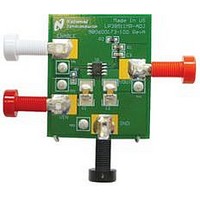
Page 4

Connection Diagram Schematic Diagram PCB Layout www.national.com 30047803 Evaluation Board Schematic. Evaluation Board Component and Pin Layout 4 30047801 30047802 ...

Page 5

Top Side Copper Area 30047811 Bottom Side Copper Area 5 www.national.com ...

Page 6

... Johnson Components Terminal; Black Terminal; Orange 125 mW; ±100 ppm; 0805 125 mW; ±100 ppm; 0805 125 mW; ±100 ppm; 0805 Diameter = 0.062” 6 Manufacturer Part Number 600173 Corporation LP38511MR-ADJ NOPB Corporation 1210ZC106KAT2A AVX 1210ZC106KAT2A KEMET C0805C332K5RAC 108-0901-001 108-0902-001 108-0903-001 108-0906-001 CRCW08051K40FK VISHAY DALE ...

Page 7

Notes 7 www.national.com ...

Page 8

... For more National Semiconductor product information and proven design tools, visit the following Web sites at: Products Amplifiers www.national.com/amplifiers Audio www.national.com/audio Clock and Timing www.national.com/timing Data Converters www.national.com/adc Interface www.national.com/interface LVDS www.national.com/lvds Power Management www.national.com/power Switching Regulators www.national.com/switchers LDOs www.national.com/ldo LED Lighting www ...

Related keywords