MCP1726EV Microchip Technology, MCP1726EV Datasheet - Page 11
MCP1726EV
Manufacturer Part Number
MCP1726EV
Description
BOARD EVAL FOR MCP1726
Manufacturer
Microchip Technology
Datasheets
1.MCP1726EV.pdf
(2 pages)
2.MCP1726EV.pdf
(30 pages)
3.MCP1726EV.pdf
(24 pages)
4.MCP1726EV.pdf
(4 pages)
5.MCP1726EV.pdf
(24 pages)
Specifications of MCP1726EV
Channels Per Ic
1 - Single
Voltage - Output
0.8 ~ 5V
Current - Output
1A
Voltage - Input
2.3 ~ 6V
Regulator Type
Positive Adjustable
Operating Temperature
-40°C ~ 125°C
Board Type
Fully Populated
Utilized Ic / Part
MCP1726
Processor To Be Evaluated
MCP1726
Silicon Manufacturer
Microchip
Silicon Core Number
MCP1726
Kit Application Type
Power Management - Voltage Regulator
Application Sub Type
LDO
Kit Contents
Board Cables CD Docs
Rohs Compliant
Yes
Lead Free Status / RoHS Status
Contains lead / RoHS non-compliant
Lead Free Status / RoHS Status
Lead free / RoHS Compliant, Contains lead / RoHS non-compliant
Available stocks
Company
Part Number
Manufacturer
Quantity
Price
Company:

Part Number:
MCP1726EV
Manufacturer:
Microchip Technology
Quantity:
135


2.1
2.2
2.3
© 2005 Microchip Technology Inc.
INTRODUCTION
FEATURES
GETTING STARTED
Chapter 2. Installation and Operation
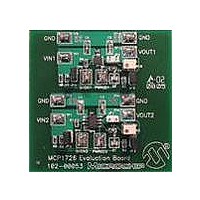
The MCP1726 1A LDO Evaluation Board demonstrates Microchip’s 1A Low-Quiescent
Current, Low-Dropout (LDO) regulator.The evaluation board contains two independent
circuits that allow the user to evaluate the MCP1726 in the 8-pin SOIC and the 8-pin
3X3 DFN packages. The evaluation board uses a potentiometer to adjust the output
voltage of the MCP1726 device across its entire output voltage range. The evaluation
board also allows for fixed-output voltage versions of the device to be used by simply
connecting the pins of a jumper connector.
The MCP1726 1A LDO Evaluation Board has the following features:
• Input Voltage Range: 2.3V to 6.0V
• Adjustable Output Voltage via a Potentiometer
• Output Voltage Shutdown via the SHDN Input
• Overcurrent Protection (device feature)
• Overtemperature Protection (device feature)
• Input Undervoltage Lockout (UVLO) Protection (device feature)
• Input Power and Power Good Indication (LED)
• Power Good Delay Adjust Capability
The MCP1726 1A LDO Evaluation Board is fully assembled and tested over its input
voltage, output voltage and output current operating range. This board requires the use
of an external input voltage source (+2.3V to +6.0V) and an external load (electronic or
resistive). The Printed Circuit Board (PCB) design provides cooling for the MCP1726
devices. When the devices are operating with high power dissipation (over 1.0W at
room ambient), additional cooling may be required to keep the devices from going into
overtemperature shutdown.
The MCP1726 1A LDO Evaluation Board contains two circuits to evaluate; one for the
SOIC package and one for the 3X3 DFN package. These circuits are powered
independently of each other through separate connectors/test points. The circuitry for
evaluating the 3X3 DFN package has inputs labeled VIN1 and SHDN1, and outputs
labeled PWRGD1 and VOUT1. The circuitry for evaluating the SOIC package has
inputs labeled VIN2 and SHDN2, and outputs labeled PWRGD2 and VOUT2. The
ground connections for the board are all common to each other and are labeled as
GND. There are a total of four connection points for ground.
All of the connections to the MCP1726 1A LDO Evaluation Board are made through
surface-mount test points. These test points can be removed with a soldering iron if you
wish to solder wires directly to the pads that are provided on the board.
MCP1726 EVALUATION
BOARD USER’S GUIDE
DS51550A-page 7
Related parts for MCP1726EV
Image
Part Number
Description
Manufacturer
Datasheet
Request
R

Part Number:
Description:
Manufacturer:
Microchip Technology Inc.
Datasheet:
Part Number:
Description:
Manufacturer:
Microchip Technology Inc.
Datasheet:
Part Number:
Description:
Manufacturer:
Microchip Technology Inc.
Datasheet:
Part Number:
Description:
Manufacturer:
Microchip Technology Inc.
Datasheet:
Part Number:
Description:
Manufacturer:
Microchip Technology Inc.
Datasheet:
Part Number:
Description:
Manufacturer:
Microchip Technology Inc.
Datasheet:
Part Number:
Description:
Manufacturer:
Microchip Technology Inc.
Datasheet:
Part Number:
Description:
Manufacturer:
Microchip Technology Inc.
Datasheet: