AS1112 EB austriamicrosystems, AS1112 EB Datasheet - Page 11
AS1112 EB
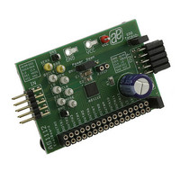
Manufacturer Part Number
AS1112 EB
Description
BOARD EVAL AS1112
Manufacturer
austriamicrosystems
Specifications of AS1112 EB
Current - Output / Channel
0.5 ~ 100 mA
Outputs And Type
16, Non-Isolated
Voltage - Output
0 ~ 15 V
Features
Over-Temperature, Open-LED, Shorted-LED, Diagnostics
Voltage - Input
3 ~ 5.5 V
Utilized Ic / Part
AS1112
Lead Free Status / RoHS Status
Lead free by exemption / RoHS compliant by exemption


AS1112
Datasheet - D e t a i l e d D e s c r i p t i o n
Power Dissipation
To ensure proper operation of the device, the total power dissipation of the AS1112 must be below the power dissipation rating of the device
package. Total power dissipation is calculated as:
Where:
V
I
V
I
DCn is the maximum dot correction value for OUTn;
n is the number of OUTn driving LED at the same time;
d
Operating Modes
The AS1112 operates in two modes
state at power-up.
Table 10. Operating Modes
Setting Dot Correction
The AS1112 can perform independent fine-adjustments to the output current of each channel, i.e., dot correction. Dot correction is used to adjust
brightness deviations of LEDs connected to the output channels (OUT0:OUT15).
The device powers up with the following default seetings: DC = 63 and GS = 4095.
The 16 channels can be individually programmed with a 6-bit word. The channel output can be adjusted in 64 steps from 0 to 100% of the maxi-
mum output current (I
Where:
I
DCn is the programmed dot correction value for output (DCn = 0 to 63);
n = 0 to 15
Dot correction data are simultaneously entered for all channels. The complete dot correction data format consists of 16 x 6-bit words, which
forms a 96-bit serial data packet
Figure 9. Dot Correction Data Packet Format
www.austriamicrosystems.com/LED-Driver-ICs/AS1112
CC
MAX
MAX
PWM
CC
OUT
is the device supply current;
is the device supply voltage;
is the LED current adjusted by R
is the maximum programmable output current for each output;
DC15.5
is the device OUTn voltage when driving LED current;
is the duty cycle defined by pin OEN or the greyscale PWM value.
MSB
95
Mode
0
1
DC OUT15
...
MAX
). The output current for each OUTn channel can be calculated as:
DC15.0
90
(see Figure
Input Shift Register
(see Table
DC14.5
IREF
89
PD = (V
192-bit
96-bit
;
9). Channel data is put on one by one, and the data is clocked in with the MSB first.
10). Greyscale operating mode
CC
x I
CC
) + (V
I
OUTn
DC OUT14:DC OUT1
OUT
= I
Revision 1.09
x I
MAX
MAX
...
x
x n x
DCn
(see Figure 12 on page 13)
63
Dot Correction Data Input Mode
DCn
63
Greyscale PWM Mode
Operating Mode
d
PWM
DC1.0
6
)
and the shift registers are in reset
DC0.5
5
DC OUT0
...
DC0.0
LSB
0
(EQ 2)
(EQ 3)
11 - 19
Related parts for AS1112 EB
Image
Part Number
Description
Manufacturer
Datasheet
Request
R

Part Number:
Description:
IC DRIVER LED 16-CHAN 32-TQFN
Manufacturer:
austriamicrosystems
Datasheet:

Part Number:
Description:
16-Channel LED Driver
Manufacturer:
austriamicrosystems AG
Datasheet:
Part Number:
Description:
IC SWITCH QUAD SPST 14-TSSOP
Manufacturer:
austriamicrosystems
Datasheet:
Part Number:
Description:
IC SWITCH QUAD SPST 14-TSSOP
Manufacturer:
austriamicrosystems
Datasheet:
Part Number:
Description:
IC AMP AUDIO MONO 1.8W 10-MSOP
Manufacturer:
austriamicrosystems
Datasheet:
Part Number:
Description:
IC AMP AUDIO MONO 1.8W 10-MSOP
Manufacturer:
austriamicrosystems
Datasheet:
Part Number:
Description:
IC AMP AUDIO MONO 1.8W 10-MSOP
Manufacturer:
austriamicrosystems
Datasheet:
Part Number:
Description:
IC AMP AUD 1.8W 3DB GAIN 10-MSOP
Manufacturer:
austriamicrosystems
Datasheet:
Part Number:
Description:
IC DRIVER LED 8-DIGIT 24-SOIC
Manufacturer:
austriamicrosystems
Datasheet:
Part Number:
Description:
IC DRIVER LED 8-DIGIT 24-SOIC
Manufacturer:
austriamicrosystems
Datasheet:
Part Number:
Description:
IC, LINE/SPEAKER PHONE CIRCUIT, SOIC-28
Manufacturer:
austriamicrosystems
Datasheet:
Part Number:
Description:
IC MULTI-STANDARD CMOS TELEPHONE SOIC-28
Manufacturer:
austriamicrosystems
Datasheet:
Part Number:
Description:
IC MULTI-STANDARD CMOS TELEPHONE SOIC-28
Manufacturer:
austriamicrosystems
Datasheet:
Part Number:
Description:
IC MULTI-STANDARD CMOS TELEPHONE SOIC-28
Manufacturer:
austriamicrosystems
Datasheet:
Part Number:
Description:
CABGA 64 (7x7)
Manufacturer:
austriamicrosystems
Datasheet: