NCP5050GEVB ON Semiconductor, NCP5050GEVB Datasheet - Page 11
NCP5050GEVB
Manufacturer Part Number
NCP5050GEVB
Description
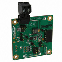
EVAL BOARD FOR NCP5050G
Manufacturer
ON Semiconductor
Specifications of NCP5050GEVB
Design Resources
NCP5050 EVB BOM NCP5050 EVB Schematic NCP5050GEVB Gerber Files
Current - Output / Channel
Adjustable
Outputs And Type
1, Non-Isolated
Voltage - Output
Up to 20V
Features
Dimmable
Voltage - Input
2.7 ~ 5.5 V
Utilized Ic / Part
NCP5050
Core Chip
NCP5050
Topology
Boost
No. Of Outputs
1
Dimming Control Type
PWM
Development Tool Type
Hardware - Eval/Demo Board
Leaded Process Compatible
Yes
Mcu Supported Families
NCP5050
Rohs Compliant
Yes
Lead Free Status / RoHS Status
Lead free / RoHS Compliant
For Use With/related Products
NCP5050G
Other names
NCP5050GEVBOS


losses in the coil and must be lower than 100 mW to limit
excessive voltage drop. In addition, as DCR is reduced,
Figure 23. Inductor Peak Currents Vs. I
Figure 22. Inductor Peak Currents Vs. I
Figure 21. Inductor Peak Currents Vs. I
3000
2500
2000
1500
1000
Finally, an acceptable DCR must be selected regarding
3000
2500
2000
1500
1000
3000
2500
2000
1500
1000
500
500
500
0
0
0
50
50
25
Switch Current Limit
Switch Current Limit
4 LEDs, (14 V @ 350 mA)
3 LEDs, (10.5 V @ 350 mA)
Setup by R
Setup by R
LEDs, (17.5 V @ 350 mA)
Switch Current Limit
75
150
Setup by R
150
PCA
PCA
PCA
I
I
125
I
out
out
out
250
Operating Inductor
(mA)
(mA)
(mA)
Peak Current
Operating Inductor
Operating Inductor
Peak Current
Peak Current
250
175
OUT
350
OUT
OUT
(mA) for 5
(mA)
(mA) for
225
http://onsemi.com
for
350
450
11
overall efficiency will improve. Some recommended
inductors include but are not limited to:
TDK VLF5012A−2R2M1R5
TDK VLF5014A−2R7M1R5
TDK RLF7030T−3R3M4R1
Switch Current Limit
allowed in the inductor according to external RPCA resistor,
which is connected between PCA input and the ground. This
allows the user to reduce the peak current being drawn
according to the application’s specific requirements. The
I
value of 2.8 kW. After selecting the switch current limit in
section above, please refer to Table 1 or Figure 24 below to
choose R
limiting the peak current to the needs of the application, the
inductor sizing can be scaled appropriately to the specific
requirements. This allows the PCB footprint to be
minimized.
Input and Output Capacitors Selection
the load during the T
stability and minimize the output ripple, at least 1.0 mF low
ESR
recommended. Increasing the C
output voltage ripple.
PEAK
Table 1. I
This safety feature is clamping the maximum current
3500
3000
2500
2000
1500
1000
C
500
OUT
0
1.0
maximum is 3.0 A, resulting in a minimum resistor
multilayer
I
stores energy during the T
PEAK_MAX
PCA
PEAK_MAX
Figure 24. I
3.0
2.5
2.0
1.5
1.0
value versus I
(A)
ceramic
Versus R
ON
PEAK_MAX
phase. In order ensure the loop
R
PCA
PEAK_MAX
10
capacitor
PCA
OUT
(kW)
OFF
vs. R
capacitor improved the
R
PCA
phase and sustains
PCA
accordingly. By
4.12
5.76
9.09
type
2.8
3.4
(kW 1%)
X5R
100
is
Related parts for NCP5050GEVB
Image
Part Number
Description
Manufacturer
Datasheet
Request
R

Part Number:
Description:
4.5 W Inductive Boost Led Driver For Flash And Lcd Backlight
Manufacturer:
ON Semiconductor
Datasheet:
Part Number:
Description:
ON Semiconductor [VOLTAGE REGULATOR]
Manufacturer:
ON Semiconductor
Datasheet:
Part Number:
Description:
357-036-542-201 CARDEDGE 36POS DL .156 BLK LOPRO
Manufacturer:
ON Semiconductor
Datasheet:
Part Number:
Description:
357-036-542-201 CARDEDGE 36POS DL .156 BLK LOPRO
Manufacturer:
ON Semiconductor
Datasheet:
Part Number:
Description:
357-036-542-201 CARDEDGE 36POS DL .156 BLK LOPRO
Manufacturer:
ON Semiconductor
Datasheet:
Part Number:
Description:
357-036-542-201 CARDEDGE 36POS DL .156 BLK LOPRO
Manufacturer:
ON Semiconductor
Datasheet:
Part Number:
Description:
357-036-542-201 CARDEDGE 36POS DL .156 BLK LOPRO
Manufacturer:
ON Semiconductor
Datasheet:
Part Number:
Description:
357-036-542-201 CARDEDGE 36POS DL .156 BLK LOPRO
Manufacturer:
ON Semiconductor
Datasheet:
Part Number:
Description:
357-036-542-201 CARDEDGE 36POS DL .156 BLK LOPRO
Manufacturer:
ON Semiconductor
Datasheet:
Part Number:
Description:
357-036-542-201 CARDEDGE 36POS DL .156 BLK LOPRO
Manufacturer:
ON Semiconductor
Datasheet:
Part Number:
Description:
357-036-542-201 CARDEDGE 36POS DL .156 BLK LOPRO
Manufacturer:
ON Semiconductor
Datasheet:
Part Number:
Description:
357-036-542-201 CARDEDGE 36POS DL .156 BLK LOPRO
Manufacturer:
ON Semiconductor
Datasheet:
Part Number:
Description:
Manufacturer:
ON Semiconductor
Datasheet:
Part Number:
Description:
Manufacturer:
ON Semiconductor
Datasheet: