NCP5005GEVB ON Semiconductor, NCP5005GEVB Datasheet - Page 7
NCP5005GEVB
Manufacturer Part Number
NCP5005GEVB
Description
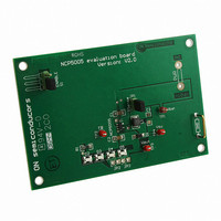
EVAL BOARD FOR NCP5005G
Manufacturer
ON Semiconductor
Specifications of NCP5005GEVB
Design Resources
NCP5005 EVB BOM NCP5005GEVB Gerber Files NCP5005 EVB Schematic
Outputs And Type
1, Non-Isolated
Voltage - Output
22V
Voltage - Input
3.6V
Utilized Ic / Part
NCP5005
Core Chip
NCP5005
Topology
Boost
No. Of Outputs
1
Development Tool Type
Hardware - Eval/Demo Board
Leaded Process Compatible
Yes
Mcu Supported Families
NCP5005SNT1G
Rohs Compliant
Yes
Lead Free Status / RoHS Status
Lead free / RoHS Compliant
Features
-
Current - Output / Channel
-
Lead Free Status / Rohs Status
Lead free / RoHS Compliant
For Use With/related Products
NCP5005G
Other names
NCP5005GEVBOS


shows a non-negligible spike when the inductor current hits
the maximum peak value (Figure 7).
for the NCP5007 application, and a similar voltage spike is
developed with 800 mVpp amplitude.
the PWM mode and the NCP5007 from a power device
standpoint, is the R
A detailed view of the PWM based chip output voltage
Basically, this is the same mechanism as the one depicted
Leaving aside the structure, the main difference between
DS(on)
Figure 7. PWM Chip Output Voltage Noise as the NMOS is Switched Off
of the internal NMOS. We have
http://onsemi.com
AND8172/D
7
1.7 W, compared to 0.5 W for the PWM chip. The
consequence is twofold:
1. With a lower R
2. Similarly, lower R
probably larger Cdg, Cgs and Cds capacitances,
thus slower dI/dt. Consequently, slower dI/dt
minimizes the effect of the parasitic inductance.
spike for the same amount of energy transferred
from the stray capacitance.
DS(on)
DS(on)
, the PWM based chip has
generates lower voltage
Related parts for NCP5005GEVB
Image
Part Number
Description
Manufacturer
Datasheet
Request
R

Part Number:
Description:
Compact Backlight LED Boost Driver
Manufacturer:
ON Semiconductor
Datasheet:
Part Number:
Description:
ON Semiconductor [VOLTAGE REGULATOR]
Manufacturer:
ON Semiconductor
Datasheet:
Part Number:
Description:
357-036-542-201 CARDEDGE 36POS DL .156 BLK LOPRO
Manufacturer:
ON Semiconductor
Datasheet:
Part Number:
Description:
357-036-542-201 CARDEDGE 36POS DL .156 BLK LOPRO
Manufacturer:
ON Semiconductor
Datasheet:
Part Number:
Description:
357-036-542-201 CARDEDGE 36POS DL .156 BLK LOPRO
Manufacturer:
ON Semiconductor
Datasheet:
Part Number:
Description:
357-036-542-201 CARDEDGE 36POS DL .156 BLK LOPRO
Manufacturer:
ON Semiconductor
Datasheet:
Part Number:
Description:
357-036-542-201 CARDEDGE 36POS DL .156 BLK LOPRO
Manufacturer:
ON Semiconductor
Datasheet:
Part Number:
Description:
357-036-542-201 CARDEDGE 36POS DL .156 BLK LOPRO
Manufacturer:
ON Semiconductor
Datasheet:
Part Number:
Description:
357-036-542-201 CARDEDGE 36POS DL .156 BLK LOPRO
Manufacturer:
ON Semiconductor
Datasheet:
Part Number:
Description:
357-036-542-201 CARDEDGE 36POS DL .156 BLK LOPRO
Manufacturer:
ON Semiconductor
Datasheet:
Part Number:
Description:
357-036-542-201 CARDEDGE 36POS DL .156 BLK LOPRO
Manufacturer:
ON Semiconductor
Datasheet:
Part Number:
Description:
357-036-542-201 CARDEDGE 36POS DL .156 BLK LOPRO
Manufacturer:
ON Semiconductor
Datasheet:
Part Number:
Description:
Manufacturer:
ON Semiconductor
Datasheet:
Part Number:
Description:
Manufacturer:
ON Semiconductor
Datasheet: