LP3944ISQEV National Semiconductor, LP3944ISQEV Datasheet - Page 6
LP3944ISQEV
Manufacturer Part Number
LP3944ISQEV
Description
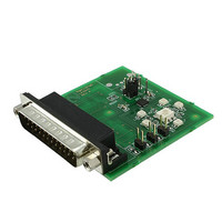
BOARD EVALUATION LP3944ISQ
Manufacturer
National Semiconductor
Series
PowerWise®r
Specifications of LP3944ISQEV
Current - Output / Channel
25mA
Outputs And Type
8, Non-Isolated
Features
Dimmable, I²C Interface
Voltage - Input
2.3 ~ 5.5 V
Utilized Ic / Part
LP3944
Core Chip
LP3944
No. Of Outputs
8
Output Current
25mA
Dimming Control Type
I2C
Kit Contents
Board, User Guide
Development Tool Type
Hardware - Eval/Demo Board
Lead Free Status / RoHS Status
Not applicable / Not applicable
Voltage - Output
-


www.national.com
Application Notes
THEORY OF OPERATION
The LP3944 takes incoming data and feed them into several
registers that control the frequency and the duty cycle of the
LEDs. Two prescaler registers and two PWM registers pro-
vide two individual rates to dim or blink the LEDs (for more
information on these registers, refer to Table 1. LP3944
REGISTER
microprocessor can program each LED to be in one of four
states — on, off, DIM0 rate or DIM1 rate. One read-only
registers provide status on all 8 LEDs. The LP3944 can be
used to drive RGB LEDs and/or single-color LEDs to create
a colorful, entertaining, and informative setting. This is par-
ticularly suitable for accessory functions in cellular phones
and toys. Any LED pins not used to drive LED can be used
for General Purpose Parallel Input/Output (GPIO) expan-
sion.
I
START and STOP bits classify the beginning and the end of
the I
transitioning from HIGH to LOW while SCL line is HIGH.
STOP condition is defined as the SDA transitioning from
LOW to HIGH while SCL is HIGH. The I
TRANSFERRING DATA
Every byte put on the SDA line must be eight bits long with
the most significant bit (MSB) being transferred first. The
number of bytes that can be transmitted per transfer is
unrestricted. Each byte of data has to be followed by an
acknowledge bit. The acknowledge related clock pulse is
generated by the master. The transmitter releases the SDA
line (HIGH) during the acknowledge clock pulse. The re-
ceiver must pull down the SDA line during the 9th clock
pulse, signifying an acknowledge. A receiver which has been
addressed must generate an acknowledge after each byte
has been received.
2
C START AND STOP CONDITIONS
2
C session. START condition is defined as SDA signal
TABLE).
The
baseband
FIGURE 2. I
2
C master always
FIGURE 1. I
controller/
2
C START and STOP Conditions
2
C Data Validity
6
The LP3944 is equipped with Power-On Reset that holds the
chip in a reset state until V
Once V
initializes itself to the default state.
To bring the LP3944 into reset, hold the RST pin LOW for a
period of TW. This will put the chip to its default state. The
LP3944 can only be programmed after RST signal is HIGH
again.
I
The data on SDA line must be stable during the HIGH period
of the clock signal (SCL). In other words, state of the data
line can only be changed when CLK is LOW.
generates START and STOP bits. The I
to be busy after START condition and free after STOP con-
dition. During data transmission, I
repeated START conditions. First START and repeated
START conditions are equivalent, function-wise.
After the START condition, a chip address is sent by the I
master. This address is seven bits long followed by an eighth
bit which is a data direction bit (R/W). The LP3944 hardwires
bits 7 to 4 and leaves bits 3 to 1 selectable, as shown in
Figure 3. For the eighth bit, a “0” indicates a WRITE and a
“1” indicates a READ. The LP3944 supports only a WRITE
during chip addressing. The second byte selects the register
to which the data will be written. The third byte contains data
to write to the selected register.
2
C DATA VALIDITY
POR
is achieved, the LP3944 comes out of reset and
20085306
20085307
DD
reaches V
2
C master can generate
POR
2
C bus is considered
during power up.
2
C
Related parts for LP3944ISQEV
Image
Part Number
Description
Manufacturer
Datasheet
Request
R

Part Number:
Description:
National Semiconductor [8-Bit D/A Converter]
Manufacturer:
National Semiconductor
Datasheet:
Part Number:
Description:
National Semiconductor [Media Coprocessor]
Manufacturer:
National Semiconductor
Datasheet:
Part Number:
Description:
Digitally Controlled Tone and Volume Circuit with Stereo Audio Power Amplifier, Microphone Preamp Stage and National 3D Sound
Manufacturer:
National Semiconductor
Datasheet:
Part Number:
Description:
Digitally Controlled Tone and Volume Circuit with Stereo Audio Power Amplifier, Microphone Preamp Stage and National 3D Sound
Manufacturer:
National Semiconductor
Datasheet:
Part Number:
Description:
AC97 Rev 2 Codec with Sample Rate Conversion and National 3D Sound
Manufacturer:
National Semiconductor
Part Number:
Description:
Manufacturer:
National Semiconductor
Datasheet:
Part Number:
Description:
Manufacturer:
National Semiconductor
Datasheet:
Part Number:
Description:
General Purpose, Low Voltage, Low Power, Rail-to-Rail Output Operational Amplifiers
Manufacturer:
National Semiconductor
Datasheet:
Part Number:
Description:
8-bit 20 MSPS flash A/D converter.
Manufacturer:
National Semiconductor
Datasheet:
Part Number:
Description:
Low Noise Quad Operational Amplifier
Manufacturer:
National Semiconductor
Datasheet:
Part Number:
Description:
Quad Differential Line Receivers
Manufacturer:
National Semiconductor
Datasheet:
Part Number:
Description:
Quad High Speed Trapezoidal? Bus Transceiver
Manufacturer:
National Semiconductor
Datasheet:
Part Number:
Description:
Dual Line Receiver
Manufacturer:
National Semiconductor
Datasheet:
Part Number:
Description:
TTL to 10k ECL Level Translator with Latch
Manufacturer:
National Semiconductor
Datasheet: