LM3502ITL-44EV National Semiconductor, LM3502ITL-44EV Datasheet - Page 2
LM3502ITL-44EV
Manufacturer Part Number
LM3502ITL-44EV
Description
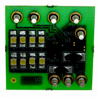
BOARD EVALUATION LM3502ITL-44
Manufacturer
National Semiconductor
Series
PowerWise®r
Specifications of LM3502ITL-44EV
Current - Output / Channel
9mA
Outputs And Type
2, Non-Isolated
Voltage - Output
44V
Features
Dual Display(s)
Voltage - Input
2.5 ~ 5.5V
Utilized Ic / Part
LM3502
Core Chip
LM3502
Topology
Boost
No. Of Outputs
1
Output Voltage
44V
Input Voltage
2.5V To 5.5V
Development Tool Type
Hardware - Eval/Demo Board
Lead Free Status / RoHS Status
Not applicable / Not applicable


www.national.com
Bump #
Connection Diagrams
Pin Descriptions/Functions
Cntrl (Bump A1): Shutdown control pin. When V
1.4V, the LM3502 is enabled or ON. When V
the LM3502 will enter into shutdown mode operation. The
LM3502 has an internal pull down resistor on the Cntrl pin,
thus the device is normally in the off state or shutdown mode
of operation.
Fb (Bump B1): Output voltage feedback connection. The
white LED string network current is set/programmed using a
resistor from this pin to ground.
V
and NMOS FET switches. (Figure 2: P1 and N2). It is rec-
ommended to connect 100nF at V
and LM3502-44 versions if V
V
FET switch (Figure 2: P1) and OVP sensing node. The
output capacitor must be connected as close to the device
OUT2
OUT1
A1
B1
C1
D1
D2
D3
C3
B3
A3
A2
(Bump D1): Source connection of the internal PMOS
(Bump C1): Drain connections of the internal PMOS
15 and 16
2 and 3
Pin #
DAP
14
13
12
10
11
9
7
6
4
1
5
8
10-Bump Thin MicroSMD
Package (TLP10)
TOP VIEW
PGND
AGND
V
V
Name
OUT2
Cntrl
DAP
En2
En1
OUT2
OUT1
Sw
V
NC
NC
NC
NC
Fb
IN
OUT2
is not used.
Shutdown Control Connection
Feedback Voltage Connection
Drain Connections of The NMOS and PMOS Field Effect Transistor (FET) Switches
(Figure 2: N2 and P1)
Over-Voltage Protection (OVP) and Source Connection of The PMOS FET Switch
(Figure 2: P1)
Drain Connection of The Power NMOS Switch (Figure 2: N1)
Power Ground Connection
Analog Ground Connection
Supply or Input Voltage Connection
NMOS FET Switch Control Connection
PMOS FET Switch Control Connection
No Connection
No Connection
No Connection
No Connection
Die Attach Pad (DAP), must be soldered to the printed circuit board’s ground plane for
enhanced thermal dissipation.
for the LM3502-35V
20131702
Cntrl
is ≤ 0.3V,
Cntrl
is ≥
2
as possible, between the V
connect the Schottky diode as close as possible to the
V
Sw (Bump D2): Drain connection of the internal power
NMOS FET switch. (Figure 2: N1) Minimize the metal trace
length and maximize the metal trace width connected to this
pin to reduce EMI radiation and trace resistance.
PGND (Bump D3): Power ground pin. Connect directly to
the ground plane.
AGND (Bump C3): Analog ground pin. Connect the analog
ground pin directly to the PGND pin.
V
C
between the V
En2 (Bump A3): Enable pin for the internal NMOS FET
switch (Figure 2: N2) during device operation. When V
OUT1
IN
IN
(Bump B3): Supply or input voltage connection pin. The
capacitor should be as close to the device as possible,
pin to minimize trace resistance and EMI radiation.
Description
16-Lead Thin Leadless Leadframe
IN
pin and ground plane.
Package (SQA16A)
TOP VIEW
OUT1
pin and ground plane. Also
20131703
En2
is
Related parts for LM3502ITL-44EV
Image
Part Number
Description
Manufacturer
Datasheet
Request
R

Part Number:
Description:
IC LED DRVR WHT BCKLT 10MICROSMD
Manufacturer:
National Semiconductor
Datasheet:
Part Number:
Description:
IC LED DRVR WHT BCKLT 10MICROSMD
Manufacturer:
National Semiconductor
Datasheet:
Part Number:
Description:
IC LED DRVR WHT BCKLT 10MICROSMD
Manufacturer:
National Semiconductor
Datasheet:
Part Number:
Description:
IC LED DRVR WHT BCKLT 10USMD
Manufacturer:
National Semiconductor
Datasheet:

Part Number:
Description:
Step-Up Converter for White LED Applications
Manufacturer:
NSC [National Semiconductor]
Datasheet:

Part Number:
Description:
National Semiconductor [8-Bit D/A Converter]
Manufacturer:
National Semiconductor
Datasheet:
Part Number:
Description:
National Semiconductor [Media Coprocessor]
Manufacturer:
National Semiconductor
Datasheet:
Part Number:
Description:
Digitally Controlled Tone and Volume Circuit with Stereo Audio Power Amplifier, Microphone Preamp Stage and National 3D Sound
Manufacturer:
National Semiconductor
Datasheet:
Part Number:
Description:
Digitally Controlled Tone and Volume Circuit with Stereo Audio Power Amplifier, Microphone Preamp Stage and National 3D Sound
Manufacturer:
National Semiconductor
Datasheet:
Part Number:
Description:
AC97 Rev 2 Codec with Sample Rate Conversion and National 3D Sound
Manufacturer:
National Semiconductor
Part Number:
Description:
Manufacturer:
National Semiconductor
Datasheet:
Part Number:
Description:
Manufacturer:
National Semiconductor
Datasheet:
Part Number:
Description:
General Purpose, Low Voltage, Low Power, Rail-to-Rail Output Operational Amplifiers
Manufacturer:
National Semiconductor
Datasheet:
Part Number:
Description:
8-bit 20 MSPS flash A/D converter.
Manufacturer:
National Semiconductor
Datasheet: