LM27961TLEV National Semiconductor, LM27961TLEV Datasheet - Page 4
LM27961TLEV
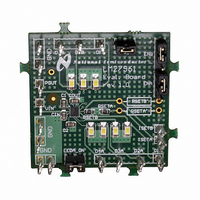
Manufacturer Part Number
LM27961TLEV
Description
BOARD EVALUATION LM27961TL
Manufacturer
National Semiconductor
Datasheet
1.LM27961TLNOPB.pdf
(13 pages)
Specifications of LM27961TLEV
Current - Output / Channel
20mA
Outputs And Type
7, Non-Isolated
Voltage - Output
4 V
Features
Charge Pump
Voltage - Input
2.7 ~ 5.5V
Utilized Ic / Part
LM27961
Lead Free Status / RoHS Status
Not applicable / Not applicable


www.national.com
R
V
f
t
1.5x/1x
Logic Pin Specifications: EN, ENA, ENB
V
V
I
SW
START
LEAK
Symbol
HR
IL
IH
OUT
Electrical Characteristics
Limits in standard typeface are for T
less otherwise specified: V
1.5V; R
pins (I
Note 1: Absolute Maximum Ratings indicate limits beyond which damage to the component may occur. Operating Ratings are conditions under which operation of
the device is guaranteed. Operating Ratings do not imply guaranteed performance limits. For guaranteed performance limits and associated test conditions, see the
Electrical Characteristics tables.
Note 2: All voltages are with respect to the potential at the GND pin.
Note 3: Internal thermal shutdown circuitry protects the device from permanent damage. Thermal shutdown engages at T
120˚C (typ.). The thermal shutdown function is guaranteed by design.
Note 4: The Human body model is a 100pF capacitor discharged through a 1.5kΩ resistor into each pin. The machine model is a 200pF capacitor discharged
directly into each pin. MIL-STD-883 3015.7
Note 5: In applications where high power dissipation and/or poor package thermal resistance is present, the maximum ambient temperature may have to be
derated. Maximum ambient temperature (T
dissipation of the device in the application (P
following equation: T
Note 6: Junction-to-ambient thermal resistance is highly dependent on application and board layout. In applications where high maximum power dissipation exists,
special care must be paid to thermal dissipation issues in board design.
Note 7: Min and Max limits are guaranteed by design, test, or statistical analysis. Typical numbers are not guaranteed, but do represent the most likely norm.
Note 8: C
Note 9: For the two groups of outputs on a part (Group A and Group B), the following are determined: the maximum output current in the group (MAX), the minimum
output current in the group (MIN), and the average output current of the group (AVG). For each group, two matching numbers are calculated: (MAX-AVG)/AVG and
(AVG-MIN)/AVG. The largest number of the two (worst case) is considered the matching figure for the group. The matching figure for a given part is considered to
be the highest matching figure of the two groups. The typical specification provided is the most likely norm of the matching figure for all parts.
Note 10: Output resistance (R
V
equation applies when the charge pump is operating with a gain of 3/2 (V
Note 11: Headroom voltage: V
Note 12: There is a 300kΩ(typ.) pull-down resistor connected internally between each enable pin (ENA, ENB) and GND.
Pout
= (1.5 x V
Dxx
SETA
IN
Charge Pump Output Resistance
(Note 10)
Current Source Headroom
Voltage Requirement (Note 11)
Switching Frequency
Start-up Time
Charge pump gain cross-over:
Gain = 1.5 when V
threshold. Gain = 1 when V
above threshold.
Input Logic Low
Input Logic High
Input Leakage Current
and I
, C
IN
POUT
= R
) – (R
SETx
A-MAX
SETB
, C
OUT
1
) apply to both Group A and Group B. (Note 8)
, and C
Parameter
= T
x I
= 8.35kΩ; C
OUT
J-MAX-OP
OUT
HR
2
IN
). In the equation, I
: Low-ESR Surface-Mount Ceramic Capacitors (MLCCs) used in setting electrical characteristics
= V
) models all voltage losses in the charge pump. R
IN
= 3.6V; V
Pout
is below
– (θ
– V
IN
JA
A-MAX
D-MAX
, C
LEDx
J
x P
IN
= 25˚C, and limits in boldface type apply over the full operating temperature range. Un-
DxA
1
) is dependent on the maximum operating junction temperature (T
is
D-MAX
, C
), and the junction-to ambient thermal resistance of the part/package in the application (θ
. If headroom voltage requirement is not met, LED current regulation will be compromised.
OUT
(Notes 2, 7) (Continued)
= 0.6V; V
2
V
I
R
(I
3.0V ≤ V
I
1.5x to 1x Threshold
1x to 1.5x Threshold
2.7V ≤ V
2.7V ≤ V
V
V
).
, and C
Dxx
Dx
is the total output current: the sum of all active Dxx output currents and all current drawn from P
Dxx
IN
ENx
ENx
SET
= 90% steady state
= 3.0V
= 95% X I
(nom) ≈ 15mA)
= 0V
= 3V (Note 12)
= 8.35kΩ
POUT
DxB
IN
IN
IN
≤ 4.2V
≤ 5.5V
≤ 5.5V
= 3.6V; ENA = 1.5V and ENB = GND, or ENA = GND and ENB =
= 1µF. Specifications related to output current(s) and current setting
IN
Dxx
≤ 4.75V typ.).
(nom)
Condition
4
OUT
can be used to estimate the voltage at the charge pump output (P
J-MAX-OP
Min
375
1.1
J
0
= 160˚C (typ.) and disengages at T
= 125˚C), the maximum power
4.75
4.55
Typ
320
500
350
2.7
0.1
10
JA
), as given by the
Max
625
0.5
V
IN
OUT
Units
OUT
. The
kHz
mV
µA
µs
Ω
V
V
V
V
J
=
):
Related parts for LM27961TLEV
Image
Part Number
Description
Manufacturer
Datasheet
Request
R

Part Number:
Description:
Accurate, 120 C-150 C Factory Preset Thermostat Lm27 Form
Manufacturer:
National Semiconductor Corporation
Datasheet:

Part Number:
Description:
Factory Preset Thermostat
Manufacturer:
National Semiconductor
Datasheet:
Part Number:
Description:
National Semiconductor [8-Bit D/A Converter]
Manufacturer:
National Semiconductor
Datasheet:
Part Number:
Description:
National Semiconductor [Media Coprocessor]
Manufacturer:
National Semiconductor
Datasheet:
Part Number:
Description:
Digitally Controlled Tone and Volume Circuit with Stereo Audio Power Amplifier, Microphone Preamp Stage and National 3D Sound
Manufacturer:
National Semiconductor
Datasheet:
Part Number:
Description:
Digitally Controlled Tone and Volume Circuit with Stereo Audio Power Amplifier, Microphone Preamp Stage and National 3D Sound
Manufacturer:
National Semiconductor
Datasheet:
Part Number:
Description:
AC97 Rev 2 Codec with Sample Rate Conversion and National 3D Sound
Manufacturer:
National Semiconductor
Part Number:
Description:
Manufacturer:
National Semiconductor
Datasheet:
Part Number:
Description:
Manufacturer:
National Semiconductor
Datasheet:
Part Number:
Description:
General Purpose, Low Voltage, Low Power, Rail-to-Rail Output Operational Amplifiers
Manufacturer:
National Semiconductor
Datasheet:
Part Number:
Description:
8-bit 20 MSPS flash A/D converter.
Manufacturer:
National Semiconductor
Datasheet:
Part Number:
Description:
Low Noise Quad Operational Amplifier
Manufacturer:
National Semiconductor
Datasheet:
Part Number:
Description:
Quad Differential Line Receivers
Manufacturer:
National Semiconductor
Datasheet:
Part Number:
Description:
Quad High Speed Trapezoidal? Bus Transceiver
Manufacturer:
National Semiconductor
Datasheet: