LX1991 EVAL KIT Microsemi Analog Mixed Signal Group, LX1991 EVAL KIT Datasheet - Page 4
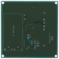
LX1991 EVAL KIT
Manufacturer Part Number
LX1991 EVAL KIT
Description
KIT EVALUATION FOR LED DRIVER
Manufacturer
Microsemi Analog Mixed Signal Group
Specifications of LX1991 EVAL KIT
Current - Output / Channel
30mA
Outputs And Type
6, Non-Isolated
Voltage - Output
40V
Features
Dimmable
Voltage - Input
4.5 ~ 5.5V
Utilized Ic / Part
LX1991
Lead Free Status / RoHS Status
Lead free / RoHS Compliant
Other names
57706
LX1991-EVAL
LX1991EVALKIT
LX1991EVALKIT
LXE1991-01 EVAL KIT
LXE1991-01EVALKIT
LXE1991-01EVALKIT
LX1991-EVAL
LX1991EVALKIT
LX1991EVALKIT
LXE1991-01 EVAL KIT
LXE1991-01EVALKIT
LXE1991-01EVALKIT


Copyright © 2001
Rev. 1.1, 10/27/2005
Unless otherwise specified, the following specifications apply over the operating ambient temperature –40°C <TA < 85°C except where otherwise noted
and with the following test conditions: V
SINK
SINK
POWER
Power Supply Input Voltage
Quiescent current
Quiescent current
Sleep Current
ENABLE INPUT
ENABLE Logic Threshold
Input Current
Input Current
OUTPUT CURRENT
SINK
I
Output Current I
Output Current DIG_DIM ≤ 0.8V
Dropout Voltage
Dropout Voltage
Maximum Output Current, I
To Gnd. Each Output
Output Off State Current
Input Current, high state
Input Current, low state
DIG_DIM to SINK
DIG_DIM to SINK
SINK
SINK
DIG_DIM Logic Threshold
Minimum SINK
CURRENT ON / OFF SLOPE
Current On rise time
Current On fall time
Current on / off delay time
RSET PIN
Voltage at Pin R
Pin R
1
2
3
SET
DIG_DIM INPUT
and 5V and R
At enable voltages greater than 0.4V but less than 0.8V the outputs will remain off but the sleep current may be greater than 1µA.
SINK
Dropout is defined as the SINK
to SINK
X
X
SET
X
X
X
TM
Current Matching
30mA
10mA
5mA
X
20mA
Max Source Current
current matching is greatest percentage delta between output currents with respect to the mean, with V
Parameter
X
1
Current Ratio
SET
X
SET
3
3
SET
Pulse Width
X
X
= 1.54KΩ.
= 0µA
Pulse Response
Pulse Response
11861 Western Avenue, Garden Grove, CA. 92841, 714-898-8121, Fax: 714-893-2570
2
SET
Shorted
X
to GND voltage at which the output current sink drops 10% from the nominal value.
DD
= 4.5 to 5.5 V
SINK
E L E C T R I C A L C H A R A C T E R I S T I C S
SINK
SINK
SINK
SINK
SINK
Symbol
SINK
V
V
I
I
I
I
I
SINK
SINK
SINK
SINK
I
IH ENABLE_
IH DIG_DIM
DD_SLEEP
IL ENABLE
IL DIG_DIM
V
V
T
I
MAX RSET
DROPOUT
DROPOUT
T
I
V
T
T
T
DD OFF
DD ON
V
TH_DD
D(OFF)
TH_EN
D(ON)
RSET
RISE
FALL
delay
DIG_DIM0
X PWMMIN
X_MATCH
DD
X_RATIO
ISETSC
SET0
X OFF
30
20
10
05
DC
, R
R
VDD = 5V, ENABLE ≥ 2.4V; DIG_DIM ≥ 2.4V
VDD = 5V, ENABLE ≥ 2.4V; DIG_DIM ≤ 0.8V
VDD = 5V, V
V
V
VDD = 5V, SINK
VDD = 5V, SINK
VDD = 5V, SINK
VDD = 5V, SINK
VDD = 5V, SINK
VDD = 5V, SINK
I
R
SINK
SINK
V
ENA ≤ 0.4V, V
V
V
C
C
C
C
C
C
SET
SET
Integrated Products
ENABLE
ENABLE
ISET
DIG_DINM
DIG_DIM
SET+
SET
SLOPE
SLOPE
SLOPE
SLOPE
SLOPE
SLOPE
®
Microsemi
= 1.54KΩ, SINK
= 0µA
= 1.02KΩ; DIG_DIM ≤ 0.8V
= Zero Volts; VDD=5V; SINK
= 1.50K to I
X
X
= 10 nF
= 10 nF
= 10 nF, T
≤ 20pF
≤ 20pF
≤ 20pF, DIG_DIM ≤ 5uS
= V
= 0V
= 10mA
= 30mA
= 0V
= V
DD
Six Output Programmable LED Current Sink
DD
OUT
Test Conditions
OUT
= 40V, ENABLE ≤ 0.4V
X
X
X
X
X
X
SET-
/I
A
= 3V, R
= 3V, R
= 3V, R
= 3V, R
= 1V to 5V; R
= 40V
SET
= 25°C
X
= 3V, DIG_DIM = 2.4V. Typical values are at T
SET
SET
SET
SET
= 1.02KΩ
= 1.54KΩ
= 3.09KΩ
= 6.19KΩ
P
SET
RODUCTION
X
= 1.54KΩ
= 5V
D
ATA
Min
28.4
1.24
4.5
0.8
0.8
19
15
15
9
4
S
SINK X
HEET
LX1991
Typ
0.08
24.5
1.26
200
600
340
230
both at 1V
3.6
1.6
0.4
1.6
0.1
4.5
10
4.0
30
20
10
±1
10
10
50
50
22
24
50
5
5
1
5
A
= 25°C
Max
1000
31.6
±2.5
1.28
100
100
800
5.5
2.4
2.4
16
10
21
11
29
29
1
1
6
3
6
LX1991
Units
mA
µSec
µSec
µSec
µA
µA
µA
mA
mA
mA
mA
mA
mA
mV
mV
mA
µA
µA
µA
µA
µA
nS
nS
µS
%
V
V
V
V
Page 4
DC
DC
DC
DC
Related parts for LX1991 EVAL KIT
Image
Part Number
Description
Manufacturer
Datasheet
Request
R

Part Number:
Description:
BOARD EVAL LED DRIVER 6 CHANNEL
Manufacturer:
Microsemi Analog Mixed Signal Group
Datasheet:

Part Number:
Description:
BOARD EVAL LED DRIVER 6CHANNEL
Manufacturer:
Microsemi Analog Mixed Signal Group
Datasheet:

Part Number:
Description:
Six Output Programmable Led Current Sink
Manufacturer:
Microsemi Corporation
Datasheet:

Part Number:
Description:
IC USB LINE TERM EMI/ESD SC70-6
Manufacturer:
Microsemi Analog Mixed Signal Group
Datasheet:
Part Number:
Description:
IC USB LINE TERM EMI/ESD SC70-6
Manufacturer:
Microsemi Analog Mixed Signal Group
Datasheet:

Part Number:
Description:
IC TERM SCSI 9LINE MODE 24TSSOP
Manufacturer:
Microsemi Analog Mixed Signal Group
Datasheet:

Part Number:
Description:
IC TERM SCSI 9LINE MODE 28TSSOP
Manufacturer:
Microsemi Analog Mixed Signal Group
Datasheet:

Part Number:
Description:
IC TERM SCSI 9LINE LVD 24TSSOP
Manufacturer:
Microsemi Analog Mixed Signal Group
Datasheet:
Part Number:
Description:
IC TERM SCSI 9LINE MODE 36QSOP
Manufacturer:
Microsemi Analog Mixed Signal Group
Datasheet:

Part Number:
Description:
IC USB LINE TERM EMI/ESD SOT23-6
Manufacturer:
Microsemi Analog Mixed Signal Group
Datasheet:

Part Number:
Description:
IC USB LINE TERM EMI/ESD SOT23-6
Manufacturer:
Microsemi Analog Mixed Signal Group
Datasheet:

Part Number:
Description:
IC USB EMI FLTR ESD PROT SOT23-6
Manufacturer:
Microsemi Analog Mixed Signal Group
Part Number:
Description:
IC USB LINE TERM EMI/ESD SOT23-6
Manufacturer:
Microsemi Analog Mixed Signal Group
Datasheet:
Part Number:
Description:
IC AMP AUDIO PWR 10W STER 44SSOP
Manufacturer:
Microsemi Analog Mixed Signal Group
Datasheet:

Part Number:
Description:
IC CHARGER BATT USB LI-ION 20MLP
Manufacturer:
Microsemi Analog Mixed Signal Group
Datasheet: