NCP5030MTTXGEVB ON Semiconductor, NCP5030MTTXGEVB Datasheet
NCP5030MTTXGEVB
Specifications of NCP5030MTTXGEVB


Related parts for NCP5030MTTXGEVB

NCP5030MTTXGEVB Summary of contents
Page 1
NCP5030 Buck-Boost Converter to Drive a Single LED from 1 Li-Ion or 3 Alkaline Batteries The NCP5030 is a fixed frequency PWM buck−boost converter optimized for constant current applications such as driving high−powered white LED. The buck−boost is implemented in ...
Page 2
VIN Osc Thermal 700 kHz Shutdown PCA 12 R1 PWM CONTROLLER CTRL Bandgap AGND ...
Page 3
PIN FUNCTION DESCRIPTION Pin Name Type 1 FB INPUT Feedback: Reference voltage is 200 mV. The cathode of the LED and a resistor to ground to set the LED current should be connected at this point. A "5% metal film ...
Page 4
MAXIMUM RATINGS (Note 1) Rating Power Supply Voltage (Note 2) Over Voltage Protection Human Body Model (HBM) ESD Rating (Note 3) Machine Model (MM) ESD Rating (Note 3) Digital Input Voltage Digital Input Current WDFN 3x4 Package Power Dissipation @ ...
Page 5
ELECTRICAL CHARACTERISTICS Characteristic Operational Power Supply Maximum Inductor Current (Note 11) (See Figure 8) Switches P1 and P2 ON Resistance Switches N1 and N2 ON Resistance Switches P1 and P2 Leakage Current Switches N1 and N2 Leakage Current Internal Oscillator ...
Page 6
TYPICAL PERFORMANCE CHARACTERISTICS 100 2.5 Figure 4. Efficiency vs. V 100 ...
Page 7
TYPICAL PERFORMANCE CHARACTERISTICS 150 100 −40 − TEMPERATURE (°C) Figure 9. NMOS R vs. Temperature DSON Figure 11. Transitional Period Switch Pins (LX1 and LX2) from ...
Page 8
DETAILED OPERATING DESCRIPTION 1.18 V Bandgap Reference and 1000 mV PCA Current Sources 12 I_SENSE THERMAL PROTECTION VIN VS IPEAK − COMP + I_SENSE + − PWM COMP ONE SHOT VIN UVLO REF RAMP COMP EXPOSED PAD 11 13 AGND ...
Page 9
Operation The NCP5030 DC−DC converter is based on a Current Mode PWM architecture specifically designed to efficiently provide a regulated current to a high current white LED. This device utilizes fixed frequency synchronous buck−boost switching regulator architecture. This topology is ...
Page 10
During this phase the switch and P2 is off. The switch current is measured by the SENSE CURRENT and added to the RAMP COMP ...
Page 11
Current Selection Figure 22 shows an application schematic to drive two selected currents I and LED + OUT V S NCP5030 200 FLASH/TORCH M1 NTHS5404 ...
Page 12
The I maximum value resulting peak in a minimum resistor value of 30 kW. Please refer to Figure page 6 to choose R PEAK_MAX ...
Page 13
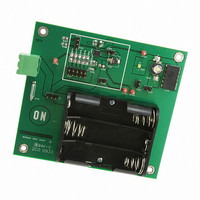
... Tape and Reel Packaging Specification Brochure, BRD8011/D. Demo Board Available: The NCP5030MTTXGEVB/D evaluation board that configures the device to drive high current through one white LED. Package WDFN12, 3x4 mm (Pb− ...
Page 14
... B NOTE 3 0.05 C *For additional information on our Pb−Free strategy and soldering details, please download the ON Semiconductor Soldering and Mounting Techniques Reference Manual, SOLDERRM/D. N. American Technical Support: 800−282−9855 Toll Free USA/Canada Europe, Middle East and Africa Technical Support: Phone: 421 33 790 2910 Japan Customer Focus Center Phone: 81− ...