LM3433SQ-36AEV/NOPB National Semiconductor, LM3433SQ-36AEV/NOPB Datasheet - Page 9
LM3433SQ-36AEV/NOPB
Manufacturer Part Number
LM3433SQ-36AEV/NOPB
Description
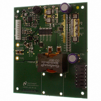
BOARD EVALUATION FOR LM3433SQ
Manufacturer
National Semiconductor
Series
PowerWise®r
Specifications of LM3433SQ-36AEV/NOPB
Current - Output / Channel
30A
Outputs And Type
1, Non-Isolated
Voltage - Output
6V
Features
Dimmable
Voltage - Input
-9 ~ -14V
Utilized Ic / Part
LM3433
Lead Free Status / RoHS Status
Lead free / RoHS Compliant
Other names
LM3433SQ-36AEV
Available stocks
Company
Part Number
Manufacturer
Quantity
Price
Company:

Part Number:
LM3433SQ-36AEV/NOPB
Manufacturer:
National Semiconductor
Quantity:
135


TIMING COMPONENTS (R
Using the calculated value for TIME
nents R
enough to dominate the parasitic capacitance of the T
A good C
culated TIME
R
INDUCTOR SELECTION
The most critical inductor parameters are inductance, current
rating, and DC resistance. To calculate the inductance, use
the desired peak to peak LED ripple current (I
and C
inductor value is calculated using the following equation:
For all V
and is only dependent on the passive external compo-
nents R
The I
an important parameter affecting the efficiency. Lower DC re-
sistance inductors are larger. A good tradeoff point between
the efficiency and the core size is letting the inductor I
equal 1% to 2% of the output power. The inductor should have
a current rating greater than the peak current for the applica-
tion. The peak current is I
POWER FET SELECTION
FETs should be chosen so that the I
1% of the total output power. Analysis shows best efficiency
with around 8mΩ of R
application. All of the switching loss is in the main switch FET.
An additional important parameter for the synchronous FET
is reverse recovery charge (Q
the transient voltages seen by the IC. A low Q
be used.
DIM FET SELECTION
Choose a DIM FET with the lowest R
cieny and low input current draw during the DIM cycle. The
output voltage during DIM will determine the switching fre-
quency. A lower output voltage results in a lower switching
frequency. If the lower frequency during DIM must be bound,
choose a FET with a higher R
quency higher during the DIM cycle.
ON
can be calculated based on the following equation:
2
ON
R loss caused by the DC resistance of the inductor is
ON
ON
. A reasonable value for I
ON
LED
, C
and C
value for most applications is 1nF. Based on cal-
ON
and V
ON
, C
, and L.
ON
ON
EE
, and the nominal V
can be selected. C
DSON
voltages, I
LED
and 15nC of gate charge for a 6A
ON
plus 1/2 I
RR
DSON
and C
). High Q
RIPPLE
RIPPLE
to force the switching fre-
2
ON
R
DSON
ON
RIPPLE
DSON
EE
)
, the timing compo-
RR
ON
is 10% of I
remains constant
and V
for maximum effi-
adversely affects
should be large
.
loss is less than
RR
RIPPLE
LED
FET should
voltages,
LED
2
), R
ON
R loss
. The
pin.
ON
,
9
BOOTSTRAP CAPACITORS
The LM3433 uses two bootstrap capacitors and a bypass ca-
pacitor on V
external FETs. A 2.2µF ceramic capacitor or larger is recom-
mended between the V
mended between the HS and BST pins. A 0.1µF is
recommended between BST2 and CGND.
SOFT-START CAPACITOR
The LM3433 integrates circuitry that, when used in conjunc-
tion with the SS pin, will slow the current ramp on start-up.
The SS pin is used to tailor the soft-start for a specific appli-
cation. A capacitor value of 0.1µF on the SS pin will yield a
12mS soft start time. For most applications soft start is not
needed.
ENABLE OPERATION
The EN pin of the LM3433 is designed so that it may be con-
trolled using a 1.6V or higher logic signal. If the enable func-
tion is not used, the EN pin may be tied to V
This pin is pulled to V
sistor.
PWM DIM OPERATION
The DIM pin of the LM3433 is designed so that it may be con-
trolled using a 1.6V or higher logic signal. The PWM frequen-
cy easily accomodates more than 40kHz dimming and can be
much faster if needed. If the PWM DIM pin is not used, tie it
to CGND or leave it open. The DIM pin is tied to CGND inter-
nally through a 100k pull down resistor.
LAYOUT CONSIDERATIONS
The LM3433 is a high performance current driver so attention
to layout details is critical to obtain maximum performance.
The most important PCB board design consideration is mini-
mizing the loop comprised by the main FET, synchronous
FET, and their associated decoupling capacitor(s). Place the
V
Place the PWM dimming/shunt FET as close to the LED as
possible. A ground plane should be used for power distribu-
tion to the power FETs. Use a star ground between the
LM3433 circuitry, the synchronous FET, and the decoupling
capacitor(s). The EP contact on the underside of the package
must be connected to V
resistor to CSN and CSP must be routed as a differential pair
directly from the resistor. A Kelvin connection is recommend-
ed. It is good practice to route the DIMO/DIMR, HS/HO, and
LO/LS lines as differential pairs. The most important PCB
board design consideration is minimizing the loop comprised
by the main FET, synchronous FET, and their associated de-
coupling capacitor(s). Optimally this loop should be orthogo-
nal to the ground plane.
CC
bypass capacitor as near as possible to the LM3433.
CC
to generate the voltages needed to drive the
IN
EE
CC
internally through a 100k pull up re-
. The two lines connecting the sense
and LS pins. A 0.47µF is recom-
IN
or left open.
www.national.com
Related parts for LM3433SQ-36AEV/NOPB
Image
Part Number
Description
Manufacturer
Datasheet
Request
R

Part Number:
Description:
IC LED DRIVER HIGH BRIGHT 24-LLP
Manufacturer:
National Semiconductor
Datasheet:

Part Number:
Description:
LM3433SQ-14A EVAL BOARD
Manufacturer:
National Semiconductor
Part Number:
Description:
BOARD, EVAL, 4A-20A, LED DVR, LM3433
Manufacturer:
National Semiconductor
Datasheet:
Part Number:
Description:
Common Anode Capable High Brightness LED Driver with High Frequency Dimming
Manufacturer:
National Semiconductor
Datasheet:
Part Number:
Description:
LM3433 Common Anode Capable High Brightness LED Driver with High Frequency Dimming; ; Qty per Container: 1
Manufacturer:
National Semiconductor
Datasheet:
Part Number:
Description:
National Semiconductor [8-Bit D/A Converter]
Manufacturer:
National Semiconductor
Datasheet:
Part Number:
Description:
National Semiconductor [Media Coprocessor]
Manufacturer:
National Semiconductor
Datasheet:
Part Number:
Description:
Digitally Controlled Tone and Volume Circuit with Stereo Audio Power Amplifier, Microphone Preamp Stage and National 3D Sound
Manufacturer:
National Semiconductor
Datasheet:
Part Number:
Description:
Digitally Controlled Tone and Volume Circuit with Stereo Audio Power Amplifier, Microphone Preamp Stage and National 3D Sound
Manufacturer:
National Semiconductor
Datasheet:
Part Number:
Description:
AC97 Rev 2 Codec with Sample Rate Conversion and National 3D Sound
Manufacturer:
National Semiconductor
Part Number:
Description:
Manufacturer:
National Semiconductor
Datasheet:
Part Number:
Description:
Manufacturer:
National Semiconductor
Datasheet:
Part Number:
Description:
General Purpose, Low Voltage, Low Power, Rail-to-Rail Output Operational Amplifiers
Manufacturer:
National Semiconductor
Datasheet:
Part Number:
Description:
8-bit 20 MSPS flash A/D converter.
Manufacturer:
National Semiconductor
Datasheet: