LM3407EVAL National Semiconductor, LM3407EVAL Datasheet - Page 9
LM3407EVAL
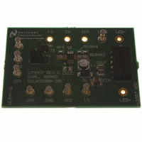
Manufacturer Part Number
LM3407EVAL
Description
BOARD EVALUATION FOR LM3407
Manufacturer
National Semiconductor
Series
PowerWise®r
Specifications of LM3407EVAL
Current - Output / Channel
350mA
Outputs And Type
1, Non-Isolated
Voltage - Output
4.5V
Features
Dimmable
Voltage - Input
4.5 ~ 30V
Utilized Ic / Part
LM3407
Lead Free Status / RoHS Status
Contains lead / RoHS non-compliant


The switching frequency and duty ratio of the converter equal:
By comparing the area of V
an error signal is generated. Such a comparison is function-
ally equivalent to comparing the middle level of I
during the ON-period of a switching cycle. The error signal is
fed to a PWM comparator circuit to produce the PWM control
pulse to drive the internal power N-MOSFET. Figure 3 shows
the implementation of the PWM switching signal. The error
signal is fed to a PWM comparator circuit to produce the PWM
control pulse to drive the internal power N-MOSFET. Figure
3 shows the implementation of the PWM switching signal.
In closed loop operation, the difference between V
V
the power switch. This behavior is independent of the induc-
tance of the inductor and input voltage because for the same
set of I
only one V
nals named V
and duty cycles but different shapes of trapezoidal wave-
forms, each generating identical PWM signals.
RP
is reflected in the changes of the switching duty cycle of
OUT
* R
MSL
ISNS
ISNS1
. Figure 4 shows two sets of current sense sig-
, ON time, and switching period, there exists
and V
ISNS2
ISNS
that have identical frequencies
and V
RP
over the ON period,
FIGURE 2. LM3407 Switching Waveforms
SNS
MSL
to V
and
RP
9
When V
switching duty cycle of the power switch will be reduced to
lower V
the switching duty cycle of the power switch will be increased
to raise V
become lower than V
regulation, the switching duty cycle of the power switch will
be increased and eventually push up V
V
to I
achieved by regulating V
of V
REF
OUT
ISNS
. Since in typical floating buck regulators V
* R
MSL
MSL
and V
MSL
FIGURE 3. Pulse-Level Transformation
ISNS
. When V
is higher than V
. For example, when I
, true average output current regulation can be
RP
under closed loop operation.
MSL
REF
is lower than the peak value of V
. In order to maintain output current
MSL
30046620
. Figure 5 shows the waveforms
REF
, the peak value of V
OUT
is decreased, V
MSL
until V
MSL
www.national.com
MSL
30046623
is equal
MSL
RP
equals
, the
will
RP
,
Related parts for LM3407EVAL
Image
Part Number
Description
Manufacturer
Datasheet
Request
R

Part Number:
Description:
Precision Fahrenheit Temperature Sensors
Manufacturer:
National Semiconductor
Part Number:
Description:
National Semiconductor [8-Bit D/A Converter]
Manufacturer:
National Semiconductor
Datasheet:
Part Number:
Description:
National Semiconductor [Media Coprocessor]
Manufacturer:
National Semiconductor
Datasheet:
Part Number:
Description:
Digitally Controlled Tone and Volume Circuit with Stereo Audio Power Amplifier, Microphone Preamp Stage and National 3D Sound
Manufacturer:
National Semiconductor
Datasheet:
Part Number:
Description:
Digitally Controlled Tone and Volume Circuit with Stereo Audio Power Amplifier, Microphone Preamp Stage and National 3D Sound
Manufacturer:
National Semiconductor
Datasheet:
Part Number:
Description:
AC97 Rev 2 Codec with Sample Rate Conversion and National 3D Sound
Manufacturer:
National Semiconductor
Part Number:
Description:
Manufacturer:
National Semiconductor
Datasheet:
Part Number:
Description:
Manufacturer:
National Semiconductor
Datasheet:
Part Number:
Description:
General Purpose, Low Voltage, Low Power, Rail-to-Rail Output Operational Amplifiers
Manufacturer:
National Semiconductor
Datasheet:
Part Number:
Description:
8-bit 20 MSPS flash A/D converter.
Manufacturer:
National Semiconductor
Datasheet:
Part Number:
Description:
Low Noise Quad Operational Amplifier
Manufacturer:
National Semiconductor
Datasheet:
Part Number:
Description:
Quad Differential Line Receivers
Manufacturer:
National Semiconductor
Datasheet:
Part Number:
Description:
Quad High Speed Trapezoidal? Bus Transceiver
Manufacturer:
National Semiconductor
Datasheet:
Part Number:
Description:
Dual Line Receiver
Manufacturer:
National Semiconductor
Datasheet: