LM3407EVAL National Semiconductor, LM3407EVAL Datasheet - Page 7
LM3407EVAL
Manufacturer Part Number
LM3407EVAL
Description
BOARD EVALUATION FOR LM3407
Manufacturer
National Semiconductor
Series
PowerWise®r
Specifications of LM3407EVAL
Current - Output / Channel
350mA
Outputs And Type
1, Non-Isolated
Voltage - Output
4.5V
Features
Dimmable
Voltage - Input
4.5 ~ 30V
Utilized Ic / Part
LM3407
Lead Free Status / RoHS Status
Contains lead / RoHS non-compliant


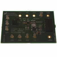
VCC, GND, EN, DIM,
PCB LAYOUT GUIDE
Since copper traces of PCBs carry resistance and parasitic
inductance, the longer the copper trace, the higher the resis-
tance and inductance. These factors introduce voltage and
current spikes to the switching nodes and impair the perfor-
mance of the whole circuit. To optimize the performance of
the LM3407, the rule of thumb is to keep the connections be-
tween components as short and direct as possible. Since true
average current regulation is achieved by detecting the aver-
age switch current, the current setting resistors RISNS1 and
RISNS2 must be located as close to the LM3407 as possible
to reduce the parasitic inductance of the copper trace and
avoid noise pick-up. The connections between LX pin, recti-
Bill of Materials
RISNS1, RISNS2
*Alternative Supplier
Designation
CIN, COUT
VIN, GND
ISNS, LX
CVCC
RFS
PCB
U1
D1
L1
J1
J2
J3
J3
Cap MLCC 50V 4.7µF X7R
Cap MLCC 10V 1.0µF X5R
LM3407 Evaluation Board
Chip Resistor 40.2kΩ 1%
Schottky Diode 40V 1.0A
Chip Resistor 1.13Ω 1%
LED Driver IC, LM3407
* Inductor 33µH 0.56A
2-way Jumper System
3-way Jumper System
Inductor 33µH 0.58A
6-pin Connector
2-pin Jumper
Description
Terminal pin
Terminal pin
4.0 x 4.0 x 1.8 (mm)
4.8 x 4.3 x 3.5 (mm)
DO-214AC (SMA)
2.54 (mm) Pitch
2.54 (mm) Pitch
2.29 (mm) Dia.
1.57 (mm) Dia.
59 x 40 (mm)
eMSOP-8
Package
DIP-12
7
1210
0805
0805
0805
fier D1, inductor L1 and output capacitor COUT should be
kept as short as possible to reduce the voltage spikes at the
LX pin. CVCC is the output filter capacitor for the internal lin-
ear regulator of the LM3407, it is recommended to be placed
close to the pin VCC. The input filter capacitor CIN should be
located close to L1 and the cathode of D1. If CIN is connected
to the VIN pin by a long trace, a 0.1µF capacitor should be
added close to pin VIN for noise filtering. In normal operation,
heat will be generated inside the LM3407 and may damage
the device if no thermal management is applied. For more
detail on switching power supply layout considerations see
Application Note AN-1149: Layout Guidelines for Switching
Power Supplies.
GRM188R61A105KA61D
GRM32ER71H475K88L
Manufacture Part #
CRCW08051R13F
CRCW08054022F
LPS4018-333ML
CR43NP-330K
535676-5
160-1026
160-1512
LM3407
SS14
Tyco Electronics
Cambion
Cambion
Coilcraft
Vendor
Sumida
Murata
Murata
Vishay
Vishay
Vishay
www.national.com
NSC
NSC
Related parts for LM3407EVAL
Image
Part Number
Description
Manufacturer
Datasheet
Request
R

Part Number:
Description:
Precision Fahrenheit Temperature Sensors
Manufacturer:
National Semiconductor
Part Number:
Description:
National Semiconductor [8-Bit D/A Converter]
Manufacturer:
National Semiconductor
Datasheet:
Part Number:
Description:
National Semiconductor [Media Coprocessor]
Manufacturer:
National Semiconductor
Datasheet:
Part Number:
Description:
Digitally Controlled Tone and Volume Circuit with Stereo Audio Power Amplifier, Microphone Preamp Stage and National 3D Sound
Manufacturer:
National Semiconductor
Datasheet:
Part Number:
Description:
Digitally Controlled Tone and Volume Circuit with Stereo Audio Power Amplifier, Microphone Preamp Stage and National 3D Sound
Manufacturer:
National Semiconductor
Datasheet:
Part Number:
Description:
AC97 Rev 2 Codec with Sample Rate Conversion and National 3D Sound
Manufacturer:
National Semiconductor
Part Number:
Description:
Manufacturer:
National Semiconductor
Datasheet:
Part Number:
Description:
Manufacturer:
National Semiconductor
Datasheet:
Part Number:
Description:
General Purpose, Low Voltage, Low Power, Rail-to-Rail Output Operational Amplifiers
Manufacturer:
National Semiconductor
Datasheet:
Part Number:
Description:
8-bit 20 MSPS flash A/D converter.
Manufacturer:
National Semiconductor
Datasheet:
Part Number:
Description:
Low Noise Quad Operational Amplifier
Manufacturer:
National Semiconductor
Datasheet:
Part Number:
Description:
Quad Differential Line Receivers
Manufacturer:
National Semiconductor
Datasheet:
Part Number:
Description:
Quad High Speed Trapezoidal? Bus Transceiver
Manufacturer:
National Semiconductor
Datasheet:
Part Number:
Description:
Dual Line Receiver
Manufacturer:
National Semiconductor
Datasheet: