551600003-001A National Semiconductor, 551600003-001A Datasheet - Page 24
551600003-001A
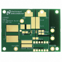
Manufacturer Part Number
551600003-001A
Description
BOARD WEBENCH MSOP LM3402
Manufacturer
National Semiconductor
Series
WEBENCH® Buildit Boardr
Datasheet
1.LM3402MMNOPB.pdf
(28 pages)
Specifications of 551600003-001A
Utilized Ic / Part
LM3402
Lead Free Status / RoHS Status
Lead free / RoHS Compliant
Features
-
Voltage - Output
-
Voltage - Input
-
Current - Output / Channel
-
Outputs And Type
-


www.national.com
In the case of a short circuit across the LED array, the
LM3402HV will continue to deliver rated current through the
short but will reduce the output voltage to equal the CS pin
voltage of 200 mV. Worst-case peak current in this condition
would be equal to:
In the case of a short at the switch node, the output, or from
the CS pin to ground the short circuit current limit will engage
at a typical peak current of 735 mA. In order to prevent in-
ductor saturation during these fault conditions the inductor’s
peak current rating must be above 735 mA. A 680 µH off-the
shelf inductor rated to 1.2A (peak) and 0.72A (average) with
a DCR of 1.1Ω will be used for the green LED array.
R
A preliminary value for R
Δi
tions for Δi
Sub-1Ω resistors are available in both 1% and 5% tolerance.
A 1%, 0.56Ω device is the closest value, and a 0.125W, 0805
size device will handle the power dissipation of 69 mW. With
the resistance selected, the average value of LED current is
re-calculated to ensure that current is within the ±5% toler-
ance requirement. From the expression for LED current ac-
curacy:
INPUT CAPACITOR
Following the calculations from the Input Capacitor section,
Δv
pacitance is:
In expectation that more capacitance will be needed to pre-
vent power supply interaction a 2.2 µF ceramic capacitor
rated to 100V with X7R dielectric in an 1812 case size will be
used. From the Design Considerations section, input rms cur-
rent is:
Ripple current ratings for 1812 size ceramic capacitors are
typically higher than 2A, more than enough for this design.
RECIRCULATING DIODE
The input voltage of 60V ±5% requires Schottky diodes with
a reverse voltage rating greater than 60V. Some manufactur-
ers provide Schottky diodes with ratings of 70, 80 or 90V;
however the next highest standard voltage rating is 100V.
SNS
I
L
F
IN(MAX)
. This value should be re-evaluated based on the calcula-
= 0.19 / 0.56 + 0.043 / 2 = 361 mA, 3% above 350 mA
Δi
F(LED-SHORT)
I
C
IN-RMS
will be 1%
F
IN(MIN)
:
I
I
F(PEAK)
L(PEAK)
= 0.35 x Sqrt(0.82 x 0.18) = 134 mA
= (0.35 x 2.7 x 10
= [(63 – 0.2) x 2.7 x 10
P-P
= 0.35 + 0.027 = 377 mA
= 0.35 + 0.156 = 506 mA
= 600 mV. The minimum required ca-
= 314 mA
SNS
was determined in selecting
P-P
-6
) / 0.6 = 1.6 µF
-6
] / 544 x 10
-6
24
Selecting a 100V rated diode provides a large safety margin
for the ringing of the switch node and also makes cross-ref-
erencing of diodes from different vendors easier.
The next parameters to be determined are the forward current
rating and case size. In this example the high duty cycle (D =
49.2 / 60 = 82%) places less thermals stress on D1 and more
on the internal power MOSFET of the LM3402. The estimated
average diode current is:
A Schottky with a forward current rating of 0.5A would be ad-
equate, however at 100V the majority of diodes have a mini-
mum forward current rating of 1A. To determine the proper
case size, the dissipation and temperature rise in D1 can be
calculated as shown in the Design Considerations section.
V
Schottky diode at 350 mA is approximately 0.65V and the
θ
calculated as:
C
The bootstrap capacitor C
capacitor with X7R dielectric. A 25V rating is appropriate for
all application circuits. The linear regulator filter capacitor C
should always be a 100 nF ceramic capacitor, also with X7R
dielectric and a 25V rating.
EFFICIENCY
To estimate the electrical efficiency of this example the power
dissipation in each current carrying element can be calculated
and summed. Electrical efficiency, η, should not be confused
with the optical efficacy of the circuit, which depends upon the
LEDs themselves.
Total output power, P
Conduction loss, P
Gate charging and VCC loss, P
regulator:
Switching loss, P
AC rms current loss, P
P
JA
D
CIN
B
P
for a small case size such as SOD-123F in a 100V, 1A
AND C
is 88°C/W. Power dissipation and temperature rise can be
C
P
P
= I
S
= (I
G
= 0.5 x 60 x 0.361 x 40 x 10
IN(rms)
= (600 x 10
F
2
F
x R
P
2
O
P
x ESR = (0.134)
= I
DSON
S
P
P
= 0.5 x V
S
I
G
F
D
T
D
, in the internal MOSFET:
x V
C
RISE
= (I
-6
) x D = (0.361
= 0.361 x 0.18 = 65 mA
= 0.065 x 0.65 = 42 mW
, in the internal MOSFET:
+ 3 x 10
O
O
IN-OP
CIN
, is calculated as:
= 0.042 x 88 = 4°C
= 0.361 x 49.2 = 17.76W
B
, in the input capacitor:
IN
should always be a 10 nF ceramic
+ f
x I
5
2
SW
F
x 3 x 10
G
x 0.006 = 0.1 mW (negligible)
x (t
, in the gate drive and linear
2
x Q
x 1.5) x 0.82 = 160 mW
-9
R
+ t
x 3 x 10
G
) x V
-9
F
) x 60 = 90 mW
) x f
IN
SW
5
= 130 mW
F
Related parts for 551600003-001A
Image
Part Number
Description
Manufacturer
Datasheet
Request
R

Part Number:
Description:
National Semiconductor [8-Bit D/A Converter]
Manufacturer:
National Semiconductor
Datasheet:
Part Number:
Description:
National Semiconductor [Media Coprocessor]
Manufacturer:
National Semiconductor
Datasheet:
Part Number:
Description:
Digitally Controlled Tone and Volume Circuit with Stereo Audio Power Amplifier, Microphone Preamp Stage and National 3D Sound
Manufacturer:
National Semiconductor
Datasheet:
Part Number:
Description:
Digitally Controlled Tone and Volume Circuit with Stereo Audio Power Amplifier, Microphone Preamp Stage and National 3D Sound
Manufacturer:
National Semiconductor
Datasheet:
Part Number:
Description:
AC97 Rev 2 Codec with Sample Rate Conversion and National 3D Sound
Manufacturer:
National Semiconductor
Part Number:
Description:
Manufacturer:
National Semiconductor
Datasheet:
Part Number:
Description:
Manufacturer:
National Semiconductor
Datasheet:
Part Number:
Description:
General Purpose, Low Voltage, Low Power, Rail-to-Rail Output Operational Amplifiers
Manufacturer:
National Semiconductor
Datasheet:
Part Number:
Description:
8-bit 20 MSPS flash A/D converter.
Manufacturer:
National Semiconductor
Datasheet:
Part Number:
Description:
Low Noise Quad Operational Amplifier
Manufacturer:
National Semiconductor
Datasheet:
Part Number:
Description:
Quad Differential Line Receivers
Manufacturer:
National Semiconductor
Datasheet:
Part Number:
Description:
Quad High Speed Trapezoidal? Bus Transceiver
Manufacturer:
National Semiconductor
Datasheet:
Part Number:
Description:
Dual Line Receiver
Manufacturer:
National Semiconductor
Datasheet:
Part Number:
Description:
TTL to 10k ECL Level Translator with Latch
Manufacturer:
National Semiconductor
Datasheet: