CDB4353 Cirrus Logic Inc, CDB4353 Datasheet - Page 20
CDB4353
Manufacturer Part Number
CDB4353
Description
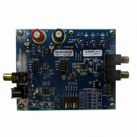
BOARD EVAL FOR CS4353 DAC
Manufacturer
Cirrus Logic Inc
Specifications of CDB4353
Number Of Dac's
2
Number Of Bits
24
Outputs And Type
2, Single Ended
Sampling Rate (per Second)
192k
Data Interface
Serial
Dac Type
Voltage
Voltage Supply Source
Single
Operating Temperature
-40°C ~ 85°C
Utilized Ic / Part
CS4353
Silicon Manufacturer
Cirrus Logic
Application Sub Type
DAC
Kit Application Type
Data Converter
Silicon Core Number
CS4353
Kit Contents
Board
Lead Free Status / RoHS Status
Contains lead / RoHS non-compliant
Lead Free Status / RoHS Status
Contains lead / RoHS non-compliant
Other names
598-1519
CDB-4353
CDB-4353


20
4.10
4.10.1 Capacitor Placement
Grounding and Power Supply Arrangements
As with any high-resolution converter, the CS4353 requires careful attention to power supply and grounding
arrangements if its potential performance is to be realized.
rangements, with VCP, VA, and VL connected to clean supplies. It is strongly recommended that a single
ground plane be used, with the DGND, CPGND, and AGND pins all connected to this common plane.
Should it be necessary to split the ground planes, the DGND and CPGND pins should be connected to the
digital ground plane and the AGND pin should be connected to the analog ground plane. In this configura-
tion, it is critical that the digital and analog ground planes be tied together with a low-impedance connection,
ideally a strip of copper on the printed circuit board, at a single point near the CS4353.
All signals, especially clocks, should be kept away from the VBIAS pin in order to avoid unwanted coupling
into the DAC.
Decoupling capacitors should be placed as close to the device as possible, with the low-value ceramic
capacitor being the closest. To further minimize impedance, these capacitors should be located on the
same PCB layer as the device. If desired, all supply pins may be connected to the same supply, but a
decoupling capacitor should still be placed on each supply pin. See
voltage present across pin pairs. This is useful for choosing appropriate capacitor voltage ratings and ori-
entation if electrolytic capacitors are used.
The CDB4353 evaluation board demonstrates the optimum layout and power supply arrangements.
Figure 3
shows the recommended power ar-
DC Electrical Characteristics
CS4353
DS803F1
for the
Related parts for CDB4353
Image
Part Number
Description
Manufacturer
Datasheet
Request
R

Part Number:
Description:
Development Kit
Manufacturer:
Cirrus Logic Inc
Datasheet:
Part Number:
Description:
Development Kit
Manufacturer:
Cirrus Logic Inc
Datasheet:


Part Number:
Description:
High-efficiency PFC + Fluorescent Lamp Driver Reference Design
Manufacturer:
Cirrus Logic Inc
Datasheet:
Part Number:
Description:
Development Kit
Manufacturer:
Cirrus Logic Inc
Datasheet:
Part Number:
Description:
Development Kit
Manufacturer:
Cirrus Logic Inc
Datasheet:

Part Number:
Description:
Development Kit
Manufacturer:
Cirrus Logic Inc
Datasheet:
Part Number:
Description:
Development Kit
Manufacturer:
Cirrus Logic Inc
Datasheet:
Part Number:
Description:
Development Kit
Manufacturer:
Cirrus Logic Inc
Datasheet:
Part Number:
Description:
Development Kit
Manufacturer:
Cirrus Logic Inc
Datasheet:

Part Number:
Description:
EVALUATION BOARD FOR CS8427
Manufacturer:
Cirrus Logic Inc
Datasheet:

Part Number:
Description:
BOARD EVAL FOR CS8416 RCVR
Manufacturer:
Cirrus Logic Inc
Datasheet:

Part Number:
Description:
EVALUATION BOARD FOR CS8420
Manufacturer:
Cirrus Logic Inc
Datasheet:

Part Number:
Description:
KIT DEVELOPMENT EP9315 ARM9
Manufacturer:
Cirrus Logic Inc
Datasheet:

Part Number:
Description:
KIT DEVELOPMENT EP9302 ARM9
Manufacturer:
Cirrus Logic Inc
Datasheet: