LM2595ADPBCKGEVB ON Semiconductor, LM2595ADPBCKGEVB Datasheet - Page 7
LM2595ADPBCKGEVB
Manufacturer Part Number
LM2595ADPBCKGEVB
Description
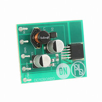
EVAL BOARD FOR LM2595ADPBCKG
Manufacturer
ON Semiconductor
Specifications of LM2595ADPBCKGEVB
Design Resources
LM2595ADPBCKGEVB BOM LM2595ADPBCKGEVB Gerber Files LM2595ADPBCKGEVB Schematic
Main Purpose
DC/DC, Step Down
Outputs And Type
1, Non-Isolated
Voltage - Output
5V
Current - Output
1A
Voltage - Input
4.5 ~ 40 V
Regulator Topology
Buck
Frequency - Switching
150kHz
Board Type
Fully Populated
Utilized Ic / Part
LM2595
Lead Free Status / RoHS Status
Lead free / RoHS Compliant
Power - Output
-
Lead Free Status / Rohs Status
Lead free / RoHS Compliant
For Use With/related Products
LM2595ADPBCKG
Other names
LM2595ADPBCKGEVBOS


B
C
D
A
1.2 A
0.6 A
1.2 A
0.6 A
10 V
0
0
0
V
A: Output Pin Voltage, 10 V/div
B: Switch Current, 0.6 A/div
C: Inductor Current, 0.6 A/div, AC−Coupled
D: Output Ripple Voltage, 50 mV/div, AC−Coupled
Horizontal Time Base: 2.0 ms/div
out
= 5 V
8.5 V - 40 V
Unregulated
Figure 14. Switching Waveforms
DC Input
TYPICAL PERFORMANCE CHARACTERISTICS
2 ms/div
C
100 mF
in
V
in
2
3
Adjustable Output Voltage Versions
GND
LM2595
Figure 16. Typical Test Circuit
5
http://onsemi.com
V out + V
R2 + R1
Where V
between 1.0 k and 5.0 k
ON/OFF
1
4
Feedback
Output
ref
ref
7
= 1.23 V, R1
V out
V
Change
Voltage
Current
ref
Output
1.0 ) R2
Load
1.0
- 100 mV
100 mV
D1
1N5822
68 mH
0.5 A
0.1 A
R1
L1
0
0
Figure 15. Load Transient Response
(Circuit of Figure 16)
C
220 mF
out
100 ms/div
R2
R1
5.0 V/1.0 A
C
FF
Load
V
out
Related parts for LM2595ADPBCKGEVB
Image
Part Number
Description
Manufacturer
Datasheet
Request
R

Part Number:
Description:
ON Semiconductor [VOLTAGE REGULATOR]
Manufacturer:
ON Semiconductor
Datasheet:
Part Number:
Description:
357-036-542-201 CARDEDGE 36POS DL .156 BLK LOPRO
Manufacturer:
ON Semiconductor
Datasheet:
Part Number:
Description:
357-036-542-201 CARDEDGE 36POS DL .156 BLK LOPRO
Manufacturer:
ON Semiconductor
Datasheet:
Part Number:
Description:
357-036-542-201 CARDEDGE 36POS DL .156 BLK LOPRO
Manufacturer:
ON Semiconductor
Datasheet:
Part Number:
Description:
357-036-542-201 CARDEDGE 36POS DL .156 BLK LOPRO
Manufacturer:
ON Semiconductor
Datasheet:
Part Number:
Description:
357-036-542-201 CARDEDGE 36POS DL .156 BLK LOPRO
Manufacturer:
ON Semiconductor
Datasheet:
Part Number:
Description:
357-036-542-201 CARDEDGE 36POS DL .156 BLK LOPRO
Manufacturer:
ON Semiconductor
Datasheet:
Part Number:
Description:
357-036-542-201 CARDEDGE 36POS DL .156 BLK LOPRO
Manufacturer:
ON Semiconductor
Datasheet:
Part Number:
Description:
357-036-542-201 CARDEDGE 36POS DL .156 BLK LOPRO
Manufacturer:
ON Semiconductor
Datasheet:
Part Number:
Description:
357-036-542-201 CARDEDGE 36POS DL .156 BLK LOPRO
Manufacturer:
ON Semiconductor
Datasheet:
Part Number:
Description:
357-036-542-201 CARDEDGE 36POS DL .156 BLK LOPRO
Manufacturer:
ON Semiconductor
Datasheet:
Part Number:
Description:
Manufacturer:
ON Semiconductor
Datasheet:
Part Number:
Description:
Manufacturer:
ON Semiconductor
Datasheet:
Part Number:
Description:
Manufacturer:
ON Semiconductor
Datasheet: