NCP1052GEVB ON Semiconductor, NCP1052GEVB Datasheet - Page 4
NCP1052GEVB
Manufacturer Part Number
NCP1052GEVB
Description
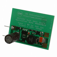
EVAL BOARD FOR NCP1052G
Manufacturer
ON Semiconductor
Specifications of NCP1052GEVB
Design Resources
NCP1052 Eval Board BOM NCP1052GEVB Gerber Files NCP1052 Demo Board Schematic
Main Purpose
AC/DC, Non-Isolated
Outputs And Type
1, Non-Isolated
Power - Output
1.2W
Voltage - Output
120V
Current - Output
100mA
Voltage - Input
85 ~ 265VAC
Regulator Topology
Boost, Buck
Frequency - Switching
136kHz
Board Type
Fully Populated
Utilized Ic / Part
NCP1052
Lead Free Status / RoHS Status
Lead free / RoHS Compliant
For Use With/related Products
NCP1052G
Other names
NCP1052GEVBOS


the circuits are mainly designed for CCM. The CCM
burst-mode waveform is different to the PWM waveform in
Figure 5. Because of this characteristic, burst mode requires
a higher peak value of the inductor current in order to have
the same level of averaged inductor current (or output
current).
low-frequency waveform comparing to the switching
frequency. Part of the power loss in this low frequency
becomes audible noise. Therefore, burst-mode control is
not suitable for high power applications such as more than
20 W.
V
circuit operate in normal mode or fault mode. The device
recognizes a fault condition when there is no feedback
current in the FB pin during the time from V
7.5 V. The V
hysteresis loop. When the circuit is in fault mode, the V
follows a 8.5 V-7.5 V-4.5 V-8.5 V hysteresis loop. The
device keeps its MOSFET opened except for the time from
V
to the output in fault mode.
startup. The MOSFET begins switching at the V
charged to 8.5 V and hence output voltage rises. The output
voltage needs some time to build up the output voltage from
0 V to a desired value. When the desired level is reached, a
feedback current flows into the device to stop its switching.
If the feedback current is determined before V
7.5V, the circuit will remain in normal mode. Otherwise, the
circuit will enter the fault mode and cannot provide the
output voltage at its desired level. Therefore, the V
capacitor is needed to be big enough to ensure sufficient time
for V
current in startup.
CC
CC
In non-isolated topologies such as buck or buck-boost,
As shown in Figure 4 and 5 burst-mode control produces
The V
In normal mode, the V
A common and extreme case to enter fault condition is the
Figure 5. CCM Inductor Currents in Burst Mode
Capacitor
= 8.5 V to 7.5 V and delivers a little amount of power
CC
CC
going from 8.5 V to 7.5 V to sample feedback
capacitor C
CC
and traditional PWM Control
capacitor directly affects this time duration.
Burst mode
2
PWM
is the key component to make the
CC
follows a 8.5 V-7.5 V-8.5 V
CC
CC
CC
= 8.5 V to
is firstly
reaches
http://onsemi.com
AND8098/D
CC
CC
4
mA in normal operation. The concerned fault sampling time
for feedback signal is from 8.5 V to 7.5V. Hence,
designed to be 20 ms, 10 F V
Inductor
with a condition that the di/dt reaches 300 mA in 4 s. When
the buck or buck-boost circuit is designed for universal ac
input voltage (85 to 265 Vac), the rectified input voltage will
be possibly as high as 375 Vdc. In order to keep the 4 s
condition, the inductance value will be 5 mH by (5) and (6).
practical. Therefore, the inductor is basically selected by
market available inductor models which is with a normally
smaller inductance (but not too small). It must have enough
saturation current level (>300 mA). If inductance is too
Practically, the NCP1052 consumes approximately 0.5
For example, if sampling time or startup transient is
The 300 mA current limit in the NCP1052 is measured
For buck,
For buck-boost,
The 5 mH is practically too high and hence not very
Figure 6. Startup Scenarios of the Circuits with
Big Enough or Too Small V
Output waveforms with big enough V
Output waveforms with too small V
C + I dt
+ 0.5
dV
di
dt
+ 0.5
+
10 - 3 · sampling time
V in * V out
dt
di
1
+
L
10 - 3
V in
CC
L
capacitor is needed.
· sampling time
[
Desired level of V
CC
V in
L
CC
Capacitor
CC
capacitor
capacitor
FB current
out
V
V
(eq. 4)
(eq. 5)
(eq. 6)
time
CC
out
time
V
V
out
CC
Related parts for NCP1052GEVB
Image
Part Number
Description
Manufacturer
Datasheet
Request
R

Part Number:
Description:
ON Semiconductor [VOLTAGE REGULATOR]
Manufacturer:
ON Semiconductor
Datasheet:
Part Number:
Description:
357-036-542-201 CARDEDGE 36POS DL .156 BLK LOPRO
Manufacturer:
ON Semiconductor
Datasheet:
Part Number:
Description:
357-036-542-201 CARDEDGE 36POS DL .156 BLK LOPRO
Manufacturer:
ON Semiconductor
Datasheet:
Part Number:
Description:
357-036-542-201 CARDEDGE 36POS DL .156 BLK LOPRO
Manufacturer:
ON Semiconductor
Datasheet:
Part Number:
Description:
357-036-542-201 CARDEDGE 36POS DL .156 BLK LOPRO
Manufacturer:
ON Semiconductor
Datasheet:
Part Number:
Description:
357-036-542-201 CARDEDGE 36POS DL .156 BLK LOPRO
Manufacturer:
ON Semiconductor
Datasheet:
Part Number:
Description:
357-036-542-201 CARDEDGE 36POS DL .156 BLK LOPRO
Manufacturer:
ON Semiconductor
Datasheet:
Part Number:
Description:
357-036-542-201 CARDEDGE 36POS DL .156 BLK LOPRO
Manufacturer:
ON Semiconductor
Datasheet:
Part Number:
Description:
357-036-542-201 CARDEDGE 36POS DL .156 BLK LOPRO
Manufacturer:
ON Semiconductor
Datasheet:
Part Number:
Description:
357-036-542-201 CARDEDGE 36POS DL .156 BLK LOPRO
Manufacturer:
ON Semiconductor
Datasheet:
Part Number:
Description:
357-036-542-201 CARDEDGE 36POS DL .156 BLK LOPRO
Manufacturer:
ON Semiconductor
Datasheet:
Part Number:
Description:
Manufacturer:
ON Semiconductor
Datasheet:
Part Number:
Description:
Manufacturer:
ON Semiconductor
Datasheet:
Part Number:
Description:
Manufacturer:
ON Semiconductor
Datasheet: