NCP1014STBUCGEVB ON Semiconductor, NCP1014STBUCGEVB Datasheet - Page 2
NCP1014STBUCGEVB
Manufacturer Part Number
NCP1014STBUCGEVB
Description
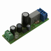
EVAL BOARD FOR NCP1014STBUCG
Manufacturer
ON Semiconductor
Datasheets
1.NCP1010ST100T3G.pdf
(24 pages)
2.NCP1014STBUCGEVB.pdf
(4 pages)
3.NCP1014STBUCGEVB.pdf
(1 pages)
Specifications of NCP1014STBUCGEVB
Design Resources
NCP1014STBUCGEVB BOM NCP1014STBUCGEVB Gerber Files NCP1014STBUCGEVB Schematic
Main Purpose
AC/DC, Non-Isolated
Outputs And Type
1, Non-Isolated
Voltage - Output
12V
Current - Output
0 ~ 3A, 0 ~ 3A, 5A
Voltage - Input
85 ~ 265VAC
Regulator Topology
Buck
Frequency - Switching
65kHz
Board Type
Fully Populated
Utilized Ic / Part
NCP1014
Lead Free Status / RoHS Status
Lead free / RoHS Compliant
Power - Output
-
Lead Free Status / Rohs Status
Lead free / RoHS Compliant
For Use With/related Products
NCP1014STBUCG
Other names
NCP1014STBUCGEVBOS


Inductor selection
minimum value of the inductance. This value is dependent
on the mode of operation. Reduced value results in
Discontinuous Conduction Mode of operation (DCM).
Practically was found, that the borderline between
Continuous Conduction Mode of operation (CCM) and
DCM is commonly set slightly below maximum output
power. The result is low cost of the inductor, freewheeling
diode (t
negative result is in lower output power and higher cost of
the NCP101x Power Switcher.
be expressed by Equation 1.
Where:
T
V
V
V
L
be expressed by Equation 2.
T
T
I
NOTE:
set
Table of Preselected Inductors (V
on
off
on
o
min
min
ds
DI ripple(Ton) + T on @
DI ripple(Toff) + T off @
I init + I set * DI ripple
For the selected output power need to be selected certain
The current ripple in the inductor during the T
The current ripple in the inductor during the T
The current through the inductor at the beginning of the
= Output Voltage,
= Peak Switching Current Set by the FB Loop.
= ON Time, Internal Power Switch in ON,
time is shown by Equation 3.
= Drain−to−Source Voltage Drop,
= OFF Time, Internal Power Switch in OFF.
= Minimum Inductor Value.
= Minimum Rectified Input Voltage,
Inductance
rr
The output current is the theoretical value and need to be multiplied by the efficiency (~0.7).
> 35 ns), higher efficiency and lower cost. The
1000
1500
(mH)
470
680
820
L min
( V min * V ds * V O )
V O
L min
min
SELECTION OF CRITICAL COMPONENTS
(see appendix for address)
Coilcraft Part Number
= 120 V, V
RFB0810−471
RFB0810−681
RFB0810−821
RFB0810−102
RFB0810−152
off
on
time may
time may
ds
http://onsemi.com
(eq. 1)
(eq. 2)
(eq. 3)
= 9 V, V
O
2
= 12 V, I
switching cycle can be expressed by Equation 4.
I
f
Equation 5.
I
Equation 6.
operation will be shown in Equation 7.
c
op_min
O
I c + f op_min @
L min +
DI ripple +
I O + f op_min @
P out_max + L min @ (I set
The average current through the inductor over one
The theoretical minimum inductor value corresponds to
The theoretical maximum output power will be shown in
The current ripple in the inductor during the normal
The output current will be shown in Equation 8.
= Inductor Operating Current,
= Output DC Current.
set
= Minimum Operating Frequency
(DI ripple
(2 @ V O @ I O @ (V min * V ds * V O ))
= 0.405 A, f
((V min * V ds ) @ f op_min @ L min )
@
((V min * V ds * V O ) @ V O )
((I set ) I init ) @ T on ) (I set ) I init ) @ T off )
(V min *V ds *V O )
2
DI
DI ripple
2 ) I init
@ f op_min @ (V min * V ds ))
(V min *V ds )
0.39
0.27
0.22
0.18
0.12
(A)
ripple
op_min
2
2
* I init
@ T on )
= 59 kHz)
2
) @ f op_min
2
2 ) I init
DI ripple
Output Current
@ T off
0.25
0.32
0.34
0.36
0.40
(A)
(eq. 4)
(eq. 5)
(eq. 6)
(eq. 7)
(eq. 8)
Related parts for NCP1014STBUCGEVB
Image
Part Number
Description
Manufacturer
Datasheet
Request
R

Part Number:
Description:
ON Semiconductor [VOLTAGE REGULATOR]
Manufacturer:
ON Semiconductor
Datasheet:
Part Number:
Description:
357-036-542-201 CARDEDGE 36POS DL .156 BLK LOPRO
Manufacturer:
ON Semiconductor
Datasheet:
Part Number:
Description:
357-036-542-201 CARDEDGE 36POS DL .156 BLK LOPRO
Manufacturer:
ON Semiconductor
Datasheet:
Part Number:
Description:
357-036-542-201 CARDEDGE 36POS DL .156 BLK LOPRO
Manufacturer:
ON Semiconductor
Datasheet:
Part Number:
Description:
357-036-542-201 CARDEDGE 36POS DL .156 BLK LOPRO
Manufacturer:
ON Semiconductor
Datasheet:
Part Number:
Description:
357-036-542-201 CARDEDGE 36POS DL .156 BLK LOPRO
Manufacturer:
ON Semiconductor
Datasheet:
Part Number:
Description:
357-036-542-201 CARDEDGE 36POS DL .156 BLK LOPRO
Manufacturer:
ON Semiconductor
Datasheet:
Part Number:
Description:
357-036-542-201 CARDEDGE 36POS DL .156 BLK LOPRO
Manufacturer:
ON Semiconductor
Datasheet:
Part Number:
Description:
357-036-542-201 CARDEDGE 36POS DL .156 BLK LOPRO
Manufacturer:
ON Semiconductor
Datasheet:
Part Number:
Description:
357-036-542-201 CARDEDGE 36POS DL .156 BLK LOPRO
Manufacturer:
ON Semiconductor
Datasheet:
Part Number:
Description:
357-036-542-201 CARDEDGE 36POS DL .156 BLK LOPRO
Manufacturer:
ON Semiconductor
Datasheet:
Part Number:
Description:
Manufacturer:
ON Semiconductor
Datasheet:
Part Number:
Description:
Manufacturer:
ON Semiconductor
Datasheet:
Part Number:
Description:
Manufacturer:
ON Semiconductor
Datasheet: