MC34063LBBEVB ON Semiconductor, MC34063LBBEVB Datasheet - Page 3
MC34063LBBEVB
Manufacturer Part Number
MC34063LBBEVB
Description
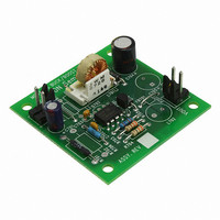
EVAL BOARD FOR MC34063LBB
Manufacturer
ON Semiconductor
Specifications of MC34063LBBEVB
Design Resources
MC34063 Demo Brd Schematic MC34063LBBEVB Gerber Files MC34063 BOM
Main Purpose
DC/DC, Step Up or Down
Outputs And Type
1, Non-Isolated
Voltage - Output
3.3V
Current - Output
100mA
Voltage - Input
3 ~ 6 V
Regulator Topology
Buck-Boost
Frequency - Switching
100kHz
Board Type
Fully Populated
Utilized Ic / Part
MC34063
Lead Free Status / RoHS Status
Lead free / RoHS Compliant
Power - Output
-
Lead Free Status / Rohs Status
Lead free / RoHS Compliant
For Use With/related Products
MC34063LBB
Other names
MC34063LBBEVBOS


4. T
5. Low duty cycle pulse techniques are used during test to maintain junction temperature as close to ambient temperature as possible.
6. If the output switch is driven into hard saturation (non−Darlington configuration) at low switch currents (≤ 300 mA) and high driver currents
* The 100 W resistor in the emitter of the driver device requires about 7.0 mA before the output switch conducts.
ELECTRICAL CHARACTERISTICS
OSCILLATOR
OUTPUT SWITCH (Note 5)
COMPARATOR
TOTAL DEVICE
Frequency (V
Charge Current (V
Discharge Current (V
Discharge to Charge Current Ratio (Pin 7 to V
Current Limit Sense Voltage (I
Saturation Voltage, Darlington Connection
Saturation Voltage (Note 6)
DC Current Gain (I
Collector Off−State Current (V
Threshold Voltage
Threshold Voltage Line Regulation (V
Input Bias Current (V
Supply Current (V
( I
V
T
(≥ 30 mA), it may take up to 2.0 ms for it to come out of saturation. This condition will shorten the off time at frequencies ≥ 30 kHz, and is
magnified at high temperatures. This condition does not occur with a Darlington configuration, since the output switch cannot saturate. If a
non−Darlington configuration is used, the following output drive condition is recommended:
Forced b of output switch :
(I
T
T
Pin 5
low
high
SW
A
A
MC33063, MC34063
MC33063V, NCV33063
SW
= 25°C
= T
= 0°C for MC34063, SC34063; − 40°C for MC33063, SC33063, MC33063V, NCV33063
= 1.0 A, Pins 1, 8 connected)
= +70°C for MC34063, SC34063; + 85°C for MC33063, SC33063; +125°C for MC33063V, NCV33063
= 1.0 A, R
> V
low
th
to T
, Pin 2 = GND, remaining pins open)
Pin 5
high
Pin 8
CC
= 0 V, C
CC
SW
in
CC
= 5.0 V to 40 V, C
= 5.0 V to 40 V, T
= 82 W to V
= 1.0 A, V
= 0 V)
= 5.0 V to 40 V, T
T
= 1.0 nF, T
I C driver – 7.0 mA *
chg
CE
Characteristics
CE
= 40 V)
= I
CC
I C output
= 5.0 V, T
dischg
, Forced b ] 20)
CC
A
T
A
= 25°C)
= 3.0 V to 40 V)
= 1.0 nF, Pin 7 = V
= 25°C)
(V
, T
A
= 25°C)
CC
A
A
CC
= 25°C)
= 25°C)
= 5.0 V, T
, T
w 10
A
= 25°C)
http://onsemi.com
A
= T
CC
low
,
to T
3
high
[Note 4], unless otherwise specified.)
I
V
dischg
Symbol
V
V
ipk(sense)
Reg
I
I
dischg
CE(sat)
CE(sat)
C(off)
f
I
h
I
V
osc
chg
I
CC
FE
IB
th
line
/I
chg
1.225
1.21
Min
140
250
5.2
24
24
50
−
−
−
−
−
−
−
0.45
0.01
1.25
−20
Typ
220
300
6.5
1.0
1.4
1.4
33
35
75
−
−
1.275
−400
Max
1.29
260
350
100
7.5
1.3
0.7
5.0
6.0
4.0
42
42
−
Unit
kHz
mV
mV
mA
nA
mA
mA
mA
V
V
V
−
−
Related parts for MC34063LBBEVB
Image
Part Number
Description
Manufacturer
Datasheet
Request
R

Part Number:
Description:
EVAL BOARD FOR MC34063LBK
Manufacturer:
ON Semiconductor
Datasheet:

Part Number:
Description:
EVAL BOARD FOR MC34063LINV
Manufacturer:
ON Semiconductor
Datasheet:

Part Number:
Description:
ON Semiconductor [VOLTAGE REGULATOR]
Manufacturer:
ON Semiconductor
Datasheet:
Part Number:
Description:
357-036-542-201 CARDEDGE 36POS DL .156 BLK LOPRO
Manufacturer:
ON Semiconductor
Datasheet:
Part Number:
Description:
357-036-542-201 CARDEDGE 36POS DL .156 BLK LOPRO
Manufacturer:
ON Semiconductor
Datasheet:
Part Number:
Description:
357-036-542-201 CARDEDGE 36POS DL .156 BLK LOPRO
Manufacturer:
ON Semiconductor
Datasheet:
Part Number:
Description:
357-036-542-201 CARDEDGE 36POS DL .156 BLK LOPRO
Manufacturer:
ON Semiconductor
Datasheet:
Part Number:
Description:
357-036-542-201 CARDEDGE 36POS DL .156 BLK LOPRO
Manufacturer:
ON Semiconductor
Datasheet:
Part Number:
Description:
357-036-542-201 CARDEDGE 36POS DL .156 BLK LOPRO
Manufacturer:
ON Semiconductor
Datasheet:
Part Number:
Description:
357-036-542-201 CARDEDGE 36POS DL .156 BLK LOPRO
Manufacturer:
ON Semiconductor
Datasheet:
Part Number:
Description:
357-036-542-201 CARDEDGE 36POS DL .156 BLK LOPRO
Manufacturer:
ON Semiconductor
Datasheet:
Part Number:
Description:
357-036-542-201 CARDEDGE 36POS DL .156 BLK LOPRO
Manufacturer:
ON Semiconductor
Datasheet:
Part Number:
Description:
357-036-542-201 CARDEDGE 36POS DL .156 BLK LOPRO
Manufacturer:
ON Semiconductor
Datasheet: