LM20143EVAL National Semiconductor, LM20143EVAL Datasheet - Page 10
LM20143EVAL
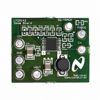
Manufacturer Part Number
LM20143EVAL
Description
BOARD EVAL 3A POWERWISE LM20143
Manufacturer
National Semiconductor
Series
PowerWise®r
Specifications of LM20143EVAL
Main Purpose
DC/DC, Step Down
Outputs And Type
1, Non-Isolated
Voltage - Output
1.2V
Current - Output
3A
Voltage - Input
2.95 ~ 5.5V
Regulator Topology
Buck
Frequency - Switching
1.5MHz
Board Type
Fully Populated
Utilized Ic / Part
LM20143
Lead Free Status / RoHS Status
Not applicable / Not applicable
Power - Output
-


www.national.com
Operation Description
GENERAL
The LM20143 switching regulator features all of the functions
necessary to implement an efficient low voltage buck regula-
tor using a minimum number of external components. This
easy to use regulator features two integrated switches and is
capable of supplying up to 3A of continuous output current.
The regulator utilizes peak current mode control with nonlin-
ear slope compensation to optimize stability and transient
response over the entire output voltage range. Peak current
mode control also provides inherent line feed-forward, cycle-
by-cycle current limiting and easy loop compensation. The
switching frequency can be varied from 500 kHz to 1.5 MHz
with an external resistor to ground. The device can operate at
high switching frequency allowing use of a small inductor
while still achieving efficiencies as high as 96%. The precision
internal voltage reference allows the output to be set as low
as 0.8V. Fault protection features include: current limiting,
thermal shutdown, over voltage protection, and shutdown ca-
pability. The device is available in the eTSSOP-16 package
featuring an exposed pad to aid thermal dissipation. The
LM20143 can be used in numerous applications to efficiently
step-down from a 5V or 3.3V bus. The typical application cir-
cuit for the LM20143 is shown in Figure 2 in the design guide.
PRECISION ENABLE
The enable (EN) pin allows the output of the device to be en-
abled or disabled with an external control signal. This pin is a
precision analog input that enables the device when the volt-
age exceeds 1.2V (typical). The EN pin has 100 mV of hys-
teresis and will disable the output when the enable voltage
falls below 1.1V (typical). If the EN pin is not used, it should
be connected to VIN. Since the enable pin has a precise turn-
on threshold it can be used along with an external resistor
divider network from V
a precise input voltage. The precision enable circuitry will re-
main active even when the device is disabled.
PEAK CURRENT MODE CONTROL
In most cases, the peak current mode control architecture
used in the LM20143 only requires two external components
to achieve a stable design. The compensation can be select-
ed to accommodate any capacitor type or value. The external
compensation also allows the user to set the crossover fre-
quency and optimize the transient performance of the device.
For duty cycles above 50% all current mode control buck
converters require the addition of an artificial ramp to avoid
sub-harmonic oscillation. This artificial linear ramp is com-
monly referred to as slope compensation. What makes the
LM20143 unique is the amount of slope compensation will
change depending on the output voltage. When operating at
high output voltages the device will have more slope com-
pensation than when operating at lower output voltages. This
is accomplished in the LM20143 by using a non-linear
parabolic ramp for the slope compensation. The parabolic
slope compensation of the LM20143 is much better than the
traditional linear slope compensation because it optimizes the
stability of the device over the entire output voltage range.
CURRENT LIMIT
The precise current limit of the LM20143 is set at the factory
to be within 10% over the entire operating temperature range.
This enables the device to operate with smaller inductors that
have lower saturation currents. When the peak inductor cur-
rent reaches the current limit threshold, an over current event
is triggered and the internal high-side FET turns off and the
IN
to configure the device to turn-on at
10
low-side FET turns on allowing the inductor current to ramp
down until the next switching cycle. For each sequential over-
current event, the reference voltage is decremented and
PWM pulses are skipped resulting in a current limit that does
not aggressively fold back for brief over-current events, while
at the same time providing frequency and voltage foldback
protection during hard short circuit conditions.
SOFT-START AND VOLTAGE TRACKING
The SS/TRK pin is a dual function pin that can be used to set
the start up time or track an external voltage source. The start
up or Soft-Start time can be adjusted by connecting a capac-
itor from the SS/TRK pin to ground. The Soft-Start feature
allows the regulator output to gradually reach the steady state
operating point, thus reducing stresses on the input supply
and controlling start up current. If no Soft-Start capacitor is
used the device defaults to the internal Soft-Start circuitry re-
sulting in a start up time of approximately 1 ms. For applica-
tions that require a monotonic start up or utilize the PGOOD
pin, an external Soft-Start capacitor is recommended. The
SS/TRK pin can also be set to track an external voltage
source. The tracking behavior can be adjusted by two external
resistors connected to the SS/TRK pin as shown in Figure 7.
in the design guide.
PRE-BIAS START UP CAPABILITY
The LM20143 is in a pre-biased state when the device starts
up with an output voltage greater than zero. This often occurs
in many multi-rail applications such as when powering an FP-
GA, ASIC, or DSP. In these applications the output can be
pre-biased through parasitic conduction paths from one sup-
ply rail to another. Even though the LM20143 is a syn-
chronous converter it will not pull the output low when a pre-
bias condition exists. During start up the LM20143 will not sink
current until the Soft-Start voltage exceeds the voltage on the
FB pin. Since the device can not sink current it protects the
load from damage that might otherwise occur if current is
conducted through the parasitic paths of the load.
POWER GOOD AND OVER VOLTAGE FAULT HANDLING
The LM20143 has built in under and over voltage compara-
tors that control the power switches. Whenever there is an
excursion in output voltage above the set OVP threshold, the
part will terminate the present on-pulse, turn-on the low-side
FET, and pull the PGOOD pin low. The low-side FET will re-
main on until either the FB voltage falls back into regulation
or the zero cross detection is triggered which in turn tri-states
the FETs. If the output reaches the UVP threshold the part will
continue switching and the PGOOD pin will be asserted and
go low. Typical values for the PGOOD resistor are on the or-
der of 100 kΩ or less. To avoid false tripping during transient
glitches the PGOOD pin has 16 µs of built in deglitch time to
both rising and falling edges.
UVLO
The LM20143 has a built-in under-voltage lockout protection
circuit that keeps the device from switching until the input
voltage reaches 2.7V (typical). The UVLO threshold has 45
mV of hysteresis that keeps the device from responding to
power-on glitches during start up. If desired the turn-on point
of the supply can be changed by using the precision enable
pin and a resistor divider network connected to V
in Figure 6. in the design guide.
THERMAL PROTECTION
Internal thermal shutdown circuitry is provided to protect the
integrated circuit in the event that the maximum junction tem-
IN
as shown
Related parts for LM20143EVAL
Image
Part Number
Description
Manufacturer
Datasheet
Request
R

Part Number:
Description:
MODULE TXRX BLUETOOTH 2 18SMD
Manufacturer:
Flexipanel
Datasheet:

Part Number:
Description:
MODULE TXRX BLUETOOTH 2 18DIP
Manufacturer:
Flexipanel
Datasheet:

Part Number:
Description:
LM20 2.4V, 10?A, SC70, micro SMD Temperature Sensor
Manufacturer:
National Semiconductor
Datasheet:
Part Number:
Description:
National Semiconductor [8-Bit D/A Converter]
Manufacturer:
National Semiconductor
Datasheet:
Part Number:
Description:
National Semiconductor [Media Coprocessor]
Manufacturer:
National Semiconductor
Datasheet:
Part Number:
Description:
Digitally Controlled Tone and Volume Circuit with Stereo Audio Power Amplifier, Microphone Preamp Stage and National 3D Sound
Manufacturer:
National Semiconductor
Datasheet:
Part Number:
Description:
Digitally Controlled Tone and Volume Circuit with Stereo Audio Power Amplifier, Microphone Preamp Stage and National 3D Sound
Manufacturer:
National Semiconductor
Datasheet:
Part Number:
Description:
AC97 Rev 2 Codec with Sample Rate Conversion and National 3D Sound
Manufacturer:
National Semiconductor
Part Number:
Description:
Manufacturer:
National Semiconductor
Datasheet:
Part Number:
Description:
Manufacturer:
National Semiconductor
Datasheet:
Part Number:
Description:
General Purpose, Low Voltage, Low Power, Rail-to-Rail Output Operational Amplifiers
Manufacturer:
National Semiconductor
Datasheet:
Part Number:
Description:
8-bit 20 MSPS flash A/D converter.
Manufacturer:
National Semiconductor
Datasheet:
Part Number:
Description:
Low Noise Quad Operational Amplifier
Manufacturer:
National Semiconductor
Datasheet:
Part Number:
Description:
Quad Differential Line Receivers
Manufacturer:
National Semiconductor
Datasheet: