MCP1630DM-DDBS1 Microchip Technology, MCP1630DM-DDBS1 Datasheet - Page 6
MCP1630DM-DDBS1
Manufacturer Part Number
MCP1630DM-DDBS1
Description
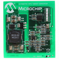
BOARD DEMO BOOST AUTO INPUT
Manufacturer
Microchip Technology
Type
DC/DC Switching Converters, Regulators & Controllersr
Specifications of MCP1630DM-DDBS1
Main Purpose
DC/DC, Step Up
Outputs And Type
1, Non-Isolated
Voltage - Output
36.5V
Current - Output
400mA
Voltage - Input
9 ~ 18V
Regulator Topology
Boost
Frequency - Switching
500kHz
Board Type
Fully Populated
Utilized Ic / Part
MCP1630
Silicon Manufacturer
Microchip
Silicon Core Number
MCP1630, PIC12F683
Core Architecture
PIC
Core Sub-architecture
PIC12
Silicon Family Name
Piccolo
Product
Power Management Modules
Lead Free Status / RoHS Status
Not applicable / Not applicable
Power - Output
-
Lead Free Status / Rohs Status
Lead free / RoHS Compliant
For Use With/related Products
MCP1630, PIC12F683
Lead Free Status / RoHS Status
Lead free / RoHS Compliant, Not applicable / Not applicable


MCP1630/MCP1630V
1.0
Absolute Maximum Ratings †
V
Maximum Voltage on Any Pin .. (V
V
Storage temperature .....................................-65°C to +150°C
Maximum Junction Temperature, T
Continuous Operating Temperature Range ..-40°C to +125°C
ESD protection on all pins, HBM
AC/DC CHARACTERISTICS
DS21896B-page 6
Electrical Specifications: Unless otherwise noted, V
V
Input Voltage
Input Operating Voltage
Input Quiescent Current
Oscillator Input
External Oscillator Range
Min. Oscillator High Time
Min. Oscillator Low Time
Oscillator Rise Time
Oscillator Fall Time
Oscillator Input Voltage Low
Oscillator Input Voltage High
Oscillator Input Capacitance
External Reference Input
Reference Voltage Input
Error Amplifier
Input Offset Voltage
Error Amplifier PSRR
Common Mode Input Range
Common Mode Rejection Ratio
Open-loop Voltage Gain
Low-level Output
Gain Bandwidth Product
Error Amplifier Sink Current
Error Amplifier Source Current
Note 1:
DD
EXT
IN
...................................................................................6.0V
for typical values = 5.0V, T
Short Circuit Current ...........................Internally Limited
2:
3:
ELECTRICAL
CHARACTERISTICS
Parameters
Capable of higher frequency operation depending on minimum and maximum duty cycles needed.
External oscillator input (OSC IN) rise and fall times between 10 ns and 10 µs used for characterization testing. Signal
levels between 0.8V and 2.0V with rise and fall times measured between 10% and 90% of maximum and minimum
values. Not production tested.
The reference input of the internal amplifier is capable of rail-to-rail operation.
A
= -40°C to +125°C.
GND
J
........................... +150°C
T
T
OH_MIN
OL_MIN
I
GBWP
SOURCE
PSRR
- 0.3)V to (V
I(V
T
T
C
F
V
Sym
A
I
V
V
V
SINK
V
RISE
FALL
V
OSC
V
OSC
REF
VOL
CM
OS
OL
IN
IN
H
L
)
GND - 0.3
IN
0.01
0.01
Min
3.0
2.0
80
85
—
—
—
—
—
—
—
+ 0.3)V
-4
-2
0
5
IN
3 kV
= 3.0V to 5.5V, F
Typ
2.8
0.1
3.5
—
—
10
—
—
—
—
—
99
—
80
95
25
11
-9
5
† Notice: Stresses above those listed under “Maximum
Ratings” may cause permanent damage to the device. This is
a stress rating only and functional operation of the device at
those or any other conditions above those indicated in the
operational listings of this specification is not implied.
Exposure to maximum rating conditions for extended periods
may affect device reliability.
AC/
GND + 50
OSC
Max
V
V
5.5
4.5
0.8
10
10
+4
—
—
—
—
—
—
—
1
IN
IN
= 1 MHz with 10% Duty Cycle, C
Units
MHz
MHz
mA
mV
mV
mA
mA
dB
dB
dB
ns
µs
µs
pf
V
V
V
V
V
V
V
I
Note 1
Note 2
Note 2
Note 2, Note 3
Note 2, Note 3
R
< V
RL = 5 k
V
V
V
V
V
EXT
IN
IN
IN
IN
COMP
IN
COMP
L
= 5 k to V
IN
© 2005 Microchip Technology Inc.
= 3.0V to 5.0V, V
= 5V, V
= 5V
= 5V, V
= 5V, V
= 0 mA, F
- 100 mV, V
= 2.0V
= 2.0V, Absolute Value
to V
CM
REF
REF
Conditions
IN
OSC IN
= 0V to 2.5V
IN
= 1.2V, V
= 1.2V, V
/2, 100 mV < V
IN
/2
CM
= 0.1 µF,
CM
= 1.2V
= 0 Hz
= 1.2V
FB
FB
= 1.4V,
= 1.0V,
EAOUT
Related parts for MCP1630DM-DDBS1
Image
Part Number
Description
Manufacturer
Datasheet
Request
R

Part Number:
Description:
BOARD CONV DEMO MCP1630 TRPL-OUT
Manufacturer:
Microchip Technology
Datasheet:

Part Number:
Description:
BOARD DEMO FOR MCP1630
Manufacturer:
Microchip Technology
Datasheet:

Part Number:
Description:
BOARD DEMO MCP1630 BIAS SUPPLY
Manufacturer:
Microchip Technology
Datasheet:

Part Number:
Description:
BOARD DEMO BOOST COUPLED INDUCTR
Manufacturer:
Microchip Technology
Datasheet:

Part Number:
Description:
BOARD DEM MCP1630 BOOST MODE LED
Manufacturer:
Microchip Technology
Datasheet:

Part Number:
Description:
Manufacturer:
Microchip Technology Inc.
Datasheet:
Part Number:
Description:
Manufacturer:
Microchip Technology Inc.
Datasheet:
Part Number:
Description:
Manufacturer:
Microchip Technology Inc.
Datasheet:
Part Number:
Description:
Manufacturer:
Microchip Technology Inc.
Datasheet:
Part Number:
Description:
Manufacturer:
Microchip Technology Inc.
Datasheet:
Part Number:
Description:
Manufacturer:
Microchip Technology Inc.
Datasheet: