NCP1203GEVB ON Semiconductor, NCP1203GEVB Datasheet - Page 3
NCP1203GEVB
Manufacturer Part Number
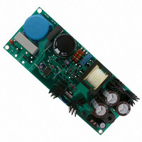
NCP1203GEVB
Description
EVAL BOARD FOR NCP1203G
Manufacturer
ON Semiconductor
Specifications of NCP1203GEVB
Design Resources
NCP1203GEVB BOM NCP1203GEVB Gerber Files NCP1203 EVB Schematic
Main Purpose
AC/DC, Primary Side
Outputs And Type
1, Isolated
Voltage - Output
19V
Current - Output
4A
Voltage - Input
85 ~ 230VAC
Regulator Topology
Flyback
Frequency - Switching
60kHz
Board Type
Fully Populated
Utilized Ic / Part
NPC1200
Lead Free Status / RoHS Status
Lead free / RoHS Compliant
Power - Output
-
Lead Free Status / Rohs Status
Lead free / RoHS Compliant
For Use With/related Products
NCP1203G
Other names
NCP1203GEVBOS


the peaks), we divide the input power by the average
rectified voltage:
Thanks to Figure 3 information, we can evaluate the
capacitor value which allows the drop from Vpeak down to
Vavg - (Vripple/2) to stay within our 50 V target, dV C =
i
(Fline = 50 Hz worse case).
Diode Bridge Selection
RMS current flowing through its internal diodes. Prior to
reach this final result, we need to evaluate the diode
conduction time. From Figure 4, we can see that the diode
starts to conduct when V
reaching Vin
time V
Vripple:
Since Vpeak is reached at the input sinusoid top (or one
fourth of the input period), then the diode conducting time
tc is simply:
load
To select the right rectifiers, it is necessary to know the
From a mathematical point of view, we can calculate the
Figure 4. When V
300 mA
Cbulk +
tc
dt:
Iload +
AC
in takes to reach Vmin, with Vmin = Vpeak -
w 171 mF or 180 mF for a normalized value
Idiode
[ 860 mA DC @ 90 VAC input voltage
peak
2 @ h @ Fline @ Vripple @ Vpeak *
Vrect avg
X-2 ms/div
V AC in @ sin(w @ t) + Vmin
:
Pin
Stops Conducting
AC
AC
in Reaches Vpeak, the Diode
+
in reaches Vmin and stops when
h @ Vpeak *
V
Pout
min
Pout
V
AC
Vripple
V
in
2
inpeak
Vbulk
Vripple
2
http://onsemi.com
AND8076/D
(1)
(2)
3
During these 3 ms, Vbulk is the seat of a rising voltage equal
to Vripple or 50 Vpp. This corresponds to a brought charge
Q of:
drawn from the input by integrating the input current over
the diode conduction time:
The expression of i
After proper integration, it comes:
If we now equate Qbulk and Qin and solve for Ipeak, it comes:
or 6 A peak. We can now evaluate the RMS current flowing
through the diodes:
rectifying function. A small resistor, or best an NTC, can
however be put in series to limit the surge current (when you
plug the SMPS in the AC outlet) to less than the diode
maximum peak current (Ifsm) or what the standard imposes
you.
at low line: 1.9 A
87.5 Watts of active power (neglecting the input diode
bridge and Cbulk losses) gives a power factor of:
conform to what we could expect from this kind of offline
power supply.
From Figure 4, we can calculate the amount of charge Q
We selected a KBU4J diode bridge (600 V/4 A) for the
Thanks to these numbers, we compute the apparent power
Irms +
Qbulk + Vripple @ Cbulk + 9 mC
tc +
[ 3 ms @ Vin + 90 VAC
+ Ipeak @
+ 1.9 A @ VAC + 90
4 @ Fline
Qin +
Qin + 1
diode
90 V = 170 VA which compared to our
PF + W
1
Ipeak @ tc * t
Ipeak +
Fline @
(t) is:
0
2
V.A
*
tc
@ Ipeak @ tc
tc
i diode (t).dt
3
sin - 1
0
@ 2 @ Fline
+ 0.51
360 @ Fline
Qbulk @ 2
tc
tc
( i diode (t) ) 2 @ dt
tc
V AC in@ 2
Vmin
(3)
(4)
(5)
(6)
(7)
(8)
(9)
Related parts for NCP1203GEVB
Image
Part Number
Description
Manufacturer
Datasheet
Request
R

Part Number:
Description:
Current Mode Controller Fixed Frequency Operation
Manufacturer:
ON Semiconductor
Datasheet:
Part Number:
Description:
ON Semiconductor [VOLTAGE REGULATOR]
Manufacturer:
ON Semiconductor
Datasheet:
Part Number:
Description:
357-036-542-201 CARDEDGE 36POS DL .156 BLK LOPRO
Manufacturer:
ON Semiconductor
Datasheet:
Part Number:
Description:
357-036-542-201 CARDEDGE 36POS DL .156 BLK LOPRO
Manufacturer:
ON Semiconductor
Datasheet:
Part Number:
Description:
357-036-542-201 CARDEDGE 36POS DL .156 BLK LOPRO
Manufacturer:
ON Semiconductor
Datasheet:
Part Number:
Description:
357-036-542-201 CARDEDGE 36POS DL .156 BLK LOPRO
Manufacturer:
ON Semiconductor
Datasheet:
Part Number:
Description:
357-036-542-201 CARDEDGE 36POS DL .156 BLK LOPRO
Manufacturer:
ON Semiconductor
Datasheet:
Part Number:
Description:
357-036-542-201 CARDEDGE 36POS DL .156 BLK LOPRO
Manufacturer:
ON Semiconductor
Datasheet:
Part Number:
Description:
357-036-542-201 CARDEDGE 36POS DL .156 BLK LOPRO
Manufacturer:
ON Semiconductor
Datasheet:
Part Number:
Description:
357-036-542-201 CARDEDGE 36POS DL .156 BLK LOPRO
Manufacturer:
ON Semiconductor
Datasheet:
Part Number:
Description:
357-036-542-201 CARDEDGE 36POS DL .156 BLK LOPRO
Manufacturer:
ON Semiconductor
Datasheet:
Part Number:
Description:
357-036-542-201 CARDEDGE 36POS DL .156 BLK LOPRO
Manufacturer:
ON Semiconductor
Datasheet:
Part Number:
Description:
Manufacturer:
ON Semiconductor
Datasheet:
Part Number:
Description:
Manufacturer:
ON Semiconductor
Datasheet: