NCP3101BUCK1GEVB ON Semiconductor, NCP3101BUCK1GEVB Datasheet - Page 18
NCP3101BUCK1GEVB
Manufacturer Part Number
NCP3101BUCK1GEVB
Description
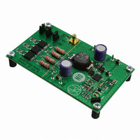
EVAL BOARD FOR NCP3101BUCK1G
Manufacturer
ON Semiconductor
Specifications of NCP3101BUCK1GEVB
Design Resources
NCP3101BUCK1 EVB BOM NCP3101BUCKL1GEVB Gerber Files NCP3101BUCK1 EVB Schematic
Main Purpose
DC/DC, Step Down
Outputs And Type
1, Non-Isolated
Voltage - Output
3.3V
Current - Output
6A
Voltage - Input
13.2V
Regulator Topology
Buck
Frequency - Switching
275kHz
Board Type
Fully Populated
Utilized Ic / Part
NCP3101
Lead Free Status / RoHS Status
Lead free / RoHS Compliant
Power - Output
-
Lead Free Status / Rohs Status
Lead free / RoHS Compliant
For Use With/related Products
NCP3101BUCK1G
Other names
NCP3101BUCK1GEVBOS


determining phase margin. To start the design, a resistor
value should be chosen for R
components can be chosen. A good starting value is 10 kW.
regulator to be adjusted down to 0.8 V via an external
resistor divider network. The regulator will maintain 0.8 V
at the feedback pin. Thus, if a resistor divider circuit was
placed across the feedback pin to V
regulate the output voltage proportional to the resistor
divider network in order to maintain 0.8 V at the FB pin.
above and the output voltage is shown in Equation 39:
R
R
V
V
The most frequently used output voltages and their
associated standard R
1
2
OUT
REF
The NCP3101C allows the output of the DC−DC
The relationship between the resistor divider network
Figure 30. Feedback Resistor Divider
= Top resistor divider
= Bottom resistor divider
= Output voltage
= Regulator reference voltage
R
2
+ R
1
1
and R
@
V
2
OUT
values are listed in Table 6.
V
2
REF
* V
from which all other
OUT
REF
, the regulator will
(eq. 39)
http://onsemi.com
18
Transconductance Error Amplifier can be calculated using
the method described below. The method serves to provide
a good starting place for compensation of a power supply.
The values can be adjusted in real time using the
compensation tool comp calc, available for download at
ON Semiconductor’s website.
follows if RF is reduced to zero.
The first pole is set at the ESR zero.
The second pole is set at zero crossover frequency.
The first zero should be set at the LC pole frequency.
The second zero is determined automatically by F
Table 6. OUTPUT VOLTAGE SETTINGS
The compensation components for the Pseudo Type III
The poles of the compensation network are calculated as
V
O
0.8
1.0
1.1
1.2
1.5
1.8
2.5
3.3
5.0
(V)
F
F
P2
F
F
P1
z1
z2
+
+
R
+
+
2p @
1
2.55
3.83
4.99
12.7
21.5
31.6
52.3
1.0
10
2p @ R
2p @ R
2p @ R
(kW)
R
R
1
1
)R
1
1
1
1
@R
C
C
1
2
@ C
@ C
@ C
2
@ C
C
F
P
F
R
Open
2
10.2
10.2
11.5
10
10
10
10
10
(kW)
P2
(eq. 40)
(eq. 41)
(eq. 42)
(eq. 43)
.
Related parts for NCP3101BUCK1GEVB
Image
Part Number
Description
Manufacturer
Datasheet
Request
R

Part Number:
Description:
Wide Input Voltage Synchronous Buck Converter
Manufacturer:
ON Semiconductor
Datasheet:
Part Number:
Description:
ON Semiconductor [VOLTAGE REGULATOR]
Manufacturer:
ON Semiconductor
Datasheet:
Part Number:
Description:
357-036-542-201 CARDEDGE 36POS DL .156 BLK LOPRO
Manufacturer:
ON Semiconductor
Datasheet:
Part Number:
Description:
357-036-542-201 CARDEDGE 36POS DL .156 BLK LOPRO
Manufacturer:
ON Semiconductor
Datasheet:
Part Number:
Description:
357-036-542-201 CARDEDGE 36POS DL .156 BLK LOPRO
Manufacturer:
ON Semiconductor
Datasheet:
Part Number:
Description:
357-036-542-201 CARDEDGE 36POS DL .156 BLK LOPRO
Manufacturer:
ON Semiconductor
Datasheet:
Part Number:
Description:
357-036-542-201 CARDEDGE 36POS DL .156 BLK LOPRO
Manufacturer:
ON Semiconductor
Datasheet:
Part Number:
Description:
357-036-542-201 CARDEDGE 36POS DL .156 BLK LOPRO
Manufacturer:
ON Semiconductor
Datasheet:
Part Number:
Description:
357-036-542-201 CARDEDGE 36POS DL .156 BLK LOPRO
Manufacturer:
ON Semiconductor
Datasheet:
Part Number:
Description:
357-036-542-201 CARDEDGE 36POS DL .156 BLK LOPRO
Manufacturer:
ON Semiconductor
Datasheet:
Part Number:
Description:
357-036-542-201 CARDEDGE 36POS DL .156 BLK LOPRO
Manufacturer:
ON Semiconductor
Datasheet:
Part Number:
Description:
357-036-542-201 CARDEDGE 36POS DL .156 BLK LOPRO
Manufacturer:
ON Semiconductor
Datasheet:
Part Number:
Description:
Manufacturer:
ON Semiconductor
Datasheet:
Part Number:
Description:
Manufacturer:
ON Semiconductor
Datasheet: