NCP1271ADAPGEVB ON Semiconductor, NCP1271ADAPGEVB Datasheet - Page 6
NCP1271ADAPGEVB
Manufacturer Part Number
NCP1271ADAPGEVB
Description
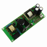
EVAL BOARD FOR NCP1271ADAPG
Manufacturer
ON Semiconductor
Datasheets
1.NCP1271P100G.pdf
(21 pages)
2.NCP1271ADAPGEVB.pdf
(1 pages)
3.NCP1271ADAPGEVB.pdf
(10 pages)
Specifications of NCP1271ADAPGEVB
Design Resources
NCP1271 Adapter EVB BOM NCP1271ADAPGEVB Gerber Files NCP1271EVB Schematic
Main Purpose
AC/DC, Primary Side
Outputs And Type
1, Isolated
Voltage - Output
19V
Current - Output
3A
Voltage - Input
85 ~ 265VAC
Regulator Topology
Flyback
Frequency - Switching
65kHz
Board Type
Fully Populated
Utilized Ic / Part
NCP1271
Silicon Manufacturer
On Semiconductor
Silicon Core Number
NCP1271
Kit Application Type
Power Management
Application Sub Type
PWM Controller
Peak Reflow Compatible (260 C)
No
Rohs Compliant
No
Lead Free Status / RoHS Status
Lead free / RoHS Compliant
Power - Output
-
Lead Free Status / Rohs Status
Lead free / RoHS Compliant
Other names
NCP1271ADAPGEVBOS


R7, is smaller than 10 kW. Now that R7 = 511 W and the
maximum allowable duty is 80% that covers the operating
duty (11.7% to 46.8% in Step 3d).
Step 4e. HV−Vcc Reverse Diode
(Pin 8). When the main power is interrupted in application,
the HV pin voltage may potentially go negative in a short
transient period. It creates a reverse current that goes out of
the HV pin and the current can damage the device. The
inserted diode turns on when the HV pin voltage goes below
the V
negative voltage on the HV pin or the reverse current.
Step 4f. Decoupling Capacitors
external decoupling capacitors.
The maximum allowable duty is 80% when ramp resistor,
The diode, D6, is a standard protection of the HV pin
There are three pins in the NCP1271 that may need
Figure 7. Transient Response with R7 = 2.0 kW
1. Skip/latch pin (Pin 1) – If the voltage on this pin is
2. Feedback pin (Pin 2) – In order to save current
3. V
CC
above 8.0 V, the circuit goes latch off. Hence, a
decoupling capacitor on this pin is essential to
increase noise immunity there.
consumption, the feedback pin sinking current in
mA−order is very easy to get polluted in a noisy
switch−mode power−supply environment and the
circuit operation may be affected.
operation when V
typical). If V
noise, the circuit wrongly recognizes it as a fault
condition. Hence, it is important to locate the V
capacitor or additional decoupling capacitor as
close as possible to the NCP1271.
biasing voltage, and hence eliminate the chance of
CC
pin (Pin 6) – The NCP1271 maintains normal
CC
drops below V
CC
is above V
CC(off)
CC(off)
by switching
(9.1 V
http://onsemi.com
AND8242/D
CC
6
Step 5. Auxiliary Supply
resistor to increase flexibility to further redesign the circuit
for other higher output voltage by dumping the extra bias
supply voltage across the resistor.
Step 6. Layout Consideration
single−layer PCB. R4 is a cancelled component in order to
save some extra standby power consumption. The major
concerns are the following.
capacitor is located exactly on the top side where the SO−7
controller is located on the bottom side. That minimizes the
Vcc pin noise that may potential lead the controller to fault
condition.
Figure 8 shows the auxiliary supply circuit. There is a
Figures 9−10 show the layout of the design. It is a
It can be observed that the electrolytic through−hole Vcc
1. To minimize the high−current loop and locate the
2. To locate the decoupling capacitors closely to the
3. To locate the V
4. To locate the output voltage sense resistor closely
5. To minimize the current sense trace that is
6. To minimize the distance between the feedback
7. To minimize the distance between the MOSFET
IC controller outside the high−current loop to
prevent malfunction of the IC internal logic due to
strong magnetic field from the high current.
device to improve noise immunity.
device to prevent the circuit enter fault condition
because of noise.
to the output load points.
low−impedance and easily polluted.
opto coupler and controller because the trace is
easily polluted.
and controller because the PCB trace is high
frequency and high current that it can easily
pollute other part of the circuit.
NCP1271
Figure 8. Auxiliary Supply
CC
C4
100uF
capacitor very close to the
R2 10
C13
100uF
Related parts for NCP1271ADAPGEVB
Image
Part Number
Description
Manufacturer
Datasheet
Request
R

Part Number:
Description:
ON Semiconductor [VOLTAGE REGULATOR]
Manufacturer:
ON Semiconductor
Datasheet:
Part Number:
Description:
357-036-542-201 CARDEDGE 36POS DL .156 BLK LOPRO
Manufacturer:
ON Semiconductor
Datasheet:
Part Number:
Description:
357-036-542-201 CARDEDGE 36POS DL .156 BLK LOPRO
Manufacturer:
ON Semiconductor
Datasheet:
Part Number:
Description:
357-036-542-201 CARDEDGE 36POS DL .156 BLK LOPRO
Manufacturer:
ON Semiconductor
Datasheet:
Part Number:
Description:
357-036-542-201 CARDEDGE 36POS DL .156 BLK LOPRO
Manufacturer:
ON Semiconductor
Datasheet:
Part Number:
Description:
357-036-542-201 CARDEDGE 36POS DL .156 BLK LOPRO
Manufacturer:
ON Semiconductor
Datasheet:
Part Number:
Description:
357-036-542-201 CARDEDGE 36POS DL .156 BLK LOPRO
Manufacturer:
ON Semiconductor
Datasheet:
Part Number:
Description:
357-036-542-201 CARDEDGE 36POS DL .156 BLK LOPRO
Manufacturer:
ON Semiconductor
Datasheet:
Part Number:
Description:
357-036-542-201 CARDEDGE 36POS DL .156 BLK LOPRO
Manufacturer:
ON Semiconductor
Datasheet:
Part Number:
Description:
357-036-542-201 CARDEDGE 36POS DL .156 BLK LOPRO
Manufacturer:
ON Semiconductor
Datasheet:
Part Number:
Description:
357-036-542-201 CARDEDGE 36POS DL .156 BLK LOPRO
Manufacturer:
ON Semiconductor
Datasheet:
Part Number:
Description:
Manufacturer:
ON Semiconductor
Datasheet:
Part Number:
Description:
Manufacturer:
ON Semiconductor
Datasheet:
Part Number:
Description:
Manufacturer:
ON Semiconductor
Datasheet: