LM5025EVAL National Semiconductor, LM5025EVAL Datasheet - Page 2
LM5025EVAL
Manufacturer Part Number
LM5025EVAL
Description
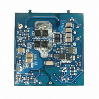
EVALUATION BOARD FOR LM5025
Manufacturer
National Semiconductor
Series
PowerWise®r
Specifications of LM5025EVAL
Main Purpose
DC/DC, Step Down
Outputs And Type
1, Non-Isolated
Voltage - Output
3.3V
Current - Output
30A
Voltage - Input
36 ~ 72V
Regulator Topology
Buck
Frequency - Switching
230kHz
Board Type
Fully Populated
Utilized Ic / Part
LM5025
Lead Free Status / RoHS Status
Contains lead / RoHS non-compliant
Power - Output
-
Other names
*LM5025EVAL
*LM5025EVAL/NOPB
LM5025EVAL
*LM5025EVAL/NOPB
LM5025EVAL


www.national.com
Connection Diagram
Ordering Information
Pin Description
PIN
Order Number
LM5025MTC
LM5025MTCX
LM5025SD
LM5025SDX
1
2
3
4
5
6
NAME
RAMP
TIME
REF
CS1
CS2
V
IN
Source Input Voltage
Modulator ramp signal
Current sense input for cycle-by-cycle limiting If CS1 exceeds 0.25V the outputs will go into
Current sense input for soft restart
Output overlap/Deadtime control
Precision 5 volt reference output
Package Type
TSSOP-16
TSSOP-16
LLP-16
LLP-16
DESCRIPTION
16-Lead TSSOP, LLP
NSC Package Drawing
MTC-16
MTC-16
SDA-16A
SDA-16A
2
Input to start-up regulator. Input range 13V to 90V,
with transient capability to 100V.
An external RC circuit from Vin sets the ramp slope.
This pin is discharged at the conclusion of every
cycle by an internal FET, initiated by either the
internal clock or the V*Sec Clamp comparator.
Cycle-by-Cycle current limit. CS1 is held low for
50ns after OUT_A switches high providing leading
edge blanking.
If CS2 exceeds 0.25V the outputs will be disabled
and a softstart commenced. The soft-start capacitor
will be fully discharged and then released with a
pull-up current of 1µA. After the first output pulse
(when SS =1V), the SS charge current will revert
back to 20µA. CS2 is held low for 50ns after OUT_A
switches high, providing leading edge blanking.
An external resistor (R
time or dead time for the active clamp output. An
R
produces in-phase OUT_A and OUT_B pulses with
overlap. An R
and REF produces out-of-phase OUT_A and OUT_B
pulses with deadtime.
Maximum output current: 10mA Locally decouple
with a 0.1µF capacitor. Reference stays low until the
line UVLO and the V
satisfied.
SET
20086916
resistor connected between TIME and GND
APPLICATION INFORMATION
SET
resistor connected between TIME
CC
Supplied As
92 Units per anti-static tube
2500 Units on Tape and Reel
1000 Units on Tape and Reel
4500 Units on Tape and Reel
SET
UV comparators are
) sets either the overlap
Related parts for LM5025EVAL
Image
Part Number
Description
Manufacturer
Datasheet
Request
R

Part Number:
Description:
Active Clamp Voltage Mode Pwm Controller
Manufacturer:
National Semiconductor Corporation
Datasheet:

Part Number:
Description:
National Semiconductor [8-Bit D/A Converter]
Manufacturer:
National Semiconductor
Datasheet:
Part Number:
Description:
National Semiconductor [Media Coprocessor]
Manufacturer:
National Semiconductor
Datasheet:
Part Number:
Description:
Digitally Controlled Tone and Volume Circuit with Stereo Audio Power Amplifier, Microphone Preamp Stage and National 3D Sound
Manufacturer:
National Semiconductor
Datasheet:
Part Number:
Description:
Digitally Controlled Tone and Volume Circuit with Stereo Audio Power Amplifier, Microphone Preamp Stage and National 3D Sound
Manufacturer:
National Semiconductor
Datasheet:
Part Number:
Description:
AC97 Rev 2 Codec with Sample Rate Conversion and National 3D Sound
Manufacturer:
National Semiconductor
Part Number:
Description:
Manufacturer:
National Semiconductor
Datasheet:
Part Number:
Description:
Manufacturer:
National Semiconductor
Datasheet:
Part Number:
Description:
General Purpose, Low Voltage, Low Power, Rail-to-Rail Output Operational Amplifiers
Manufacturer:
National Semiconductor
Datasheet:
Part Number:
Description:
8-bit 20 MSPS flash A/D converter.
Manufacturer:
National Semiconductor
Datasheet:
Part Number:
Description:
Low Noise Quad Operational Amplifier
Manufacturer:
National Semiconductor
Datasheet:
Part Number:
Description:
Quad Differential Line Receivers
Manufacturer:
National Semiconductor
Datasheet:
Part Number:
Description:
Quad High Speed Trapezoidal? Bus Transceiver
Manufacturer:
National Semiconductor
Datasheet:
Part Number:
Description:
Dual Line Receiver
Manufacturer:
National Semiconductor
Datasheet: