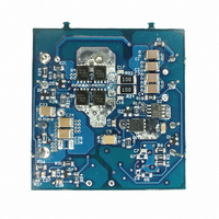
LM5025EVAL National Semiconductor, LM5025EVAL Datasheet - Page 4

LM5025EVAL
Manufacturer Part Number
LM5025EVAL
Description
EVALUATION BOARD FOR LM5025
Manufacturer
National Semiconductor
Series
PowerWise®r
Specifications of LM5025EVAL
Main Purpose
DC/DC, Step Down
Outputs And Type
1, Non-Isolated
Voltage - Output
3.3V
Current - Output
30A
Voltage - Input
36 ~ 72V
Regulator Topology
Buck
Frequency - Switching
230kHz
Board Type
Fully Populated
Utilized Ic / Part
LM5025
Lead Free Status / RoHS Status
Contains lead / RoHS non-compliant
Power - Output
-
Other names
*LM5025EVAL
*LM5025EVAL/NOPB
LM5025EVAL
*LM5025EVAL/NOPB
LM5025EVAL
www.national.com
Performance Characteristics
TURN-ON WAVEFORMS
When applying power to the LM5025A evaluation board a
certain sequence of events must occur. Soft-start capacitor
values and other components allow the feedback loop to
stabilize without overshoot. Figure 1 shows the output volt-
age during a typical start-up with a 48V input and a load of
5A. There is no overshoot during startup.
OUTPUT RIPPLE WAVEFORMS
Figure 2 shows the transient response for a load of change
from 5A to 25A. The upper trace shows output voltage droop
and overshoot during the sudden change in output current
shown by the lower trace.
Conditions: Input Voltage = 48VDC Output Current = 5A
Trace 1: Output Voltage Volts/div = 0.5V
Horizontal Resolution = 1msec/div
Conditions: Input Voltage = 48VDC Output Current = 5A to 25A
Trace 1: Output Voltage Volts/div = 0.5V
Trace 2: Output Current, Amps/div = 10.0A
Horizontal Resolution = 1µs/div
FIGURE 1.
FIGURE 2.
20127607
20127608
4
Conditions: Input Voltage = 48VDC
Output Current = 30A
Bandwidth Limit = 25MHz
Trace 1: Output Ripple Voltage Volts/div = 50mV
Horizontal Resolution = 2µs/div
Figure 3 shows typical output ripple seen directly across the
output capacitor, for an input voltage of 48V and a load of
30A. This waveform is typical of most loads and input volt-
ages.
Figure 4 and Figure 5 show the drain voltage of Q1 with a
25A load. Figure 4 represents an input voltage of 38V and
Figure 5 represents an input voltage of 78V.
Figure 6 shows the gate voltages of the synchronous recti-
fiers. The drive from the main power transformer is delayed
slightly at turn-on by a resistor interacting with the gate
capacitance. This provides improved switching transitions
for optimum efficiency. The difference in drive voltage is
inherent in the topology and varies with line voltage.
Conditions: Input Voltage = 38VDC Output Current = 25A
Trace 1: Q1 drain voltage Volts/div = 20V Horizontal Resolution = 1µs/div
FIGURE 3.
FIGURE 4.
20127609
20127604


