LM5030EVAL National Semiconductor, LM5030EVAL Datasheet - Page 3
LM5030EVAL
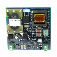
Manufacturer Part Number
LM5030EVAL
Description
EVALUATION BOARD FOR LM5030
Manufacturer
National Semiconductor
Series
PowerWise®r
Specifications of LM5030EVAL
Main Purpose
DC/DC, Step Down
Outputs And Type
1, Isolated
Voltage - Output
3.3V
Current - Output
10A
Voltage - Input
36 ~ 75V
Regulator Topology
Buck
Board Type
Fully Populated
Utilized Ic / Part
LM5030
Lead Free Status / RoHS Status
Not applicable / Not applicable
Power - Output
-
Frequency - Switching
-
Other names
*LM5030EVAL


Performance
current, the output will be regulated to within 5 mV as the
input voltage is varied over its range (36 - 75V). The power
conversion efficiency is shown in Figure 3.
Waveforms
If the circuit is to be probed, Figure 4 shows some of the
significant waveforms for various input/output combinations.
REMEMBER that there are two circuit grounds, and the
scope probe grounds must be connected appropriately.
In the table of Figure 4, t1 and t2 are in microseconds, while
Fs is in kHz. Fs is the frequency of the internal oscillator,
which is twice the switching frequency of each MOSFET. All
the voltages are in volts with respect to circuit ground. L2
Output is the regulated output at J2, and typically has less
than 10mV of ripple. The spikes at the rising edges of V4,
V5, V7, and V9 are due to the leakage inductance in T1. The
voltage rating of the MOSFETs (Q1, Q2) is determined by
the amplitude of these spikes (V4). Their current rating is
determined by the input current shown in Figure 2, plus a
ripple component of approximately 10% in this design.
V
While the LM5030 internally generates a voltage at V
(7.7V), the internal regulator is used mainly during the
start-up sequence. Once the load current begins flowing
through L2, which is both an inductor for the output filter and
a transformer, a voltage is generated at L2’s secondary
which powers the V
age exceeds the internal value (7.7V), the internal regulator
shuts off, thereby reducing internal power dissipation in the
LM5030. L2 is constructed such that the voltage supplied to
V
11.3V, depending on the load current. See Figure 5.
Current Sense
Monitoring the input current provides a good indication of the
circuit’s operation. If an overload condition should exist at
the output (a partial overload or a short circuit), the input
CC
CC
ranges from approximately 10.6V to approximately
CC
pin. Once the externally applied volt-
(Continued)
FIGURE 2. Input Current vs Load Current and V
CC
3
current would rise above the nominal value shown in Figure
2. Transformer T2, in conjunction with D3, R9, R12 and C10,
provides a voltage to pin 8 on the LM5030 (CS) which is
representative of the input current flowing through its pri-
mary. The average voltage seen at pin 8 is plotted in Figure
6. If the voltage at the first current sense comparator ex-
ceeds 0.5V, the LM5030 disables its outputs, and the circuit
enters a cycle-by-cycle current limit mode. If the second
level threshold (0.625V) is exceeded due to a severe over-
load and tranformer saturation, the LM5030 will disable its
outputs and initiate a softstart sequence. However, the very
short propagation delay of the cycle-by-cycle current limiter
(CS1), the design of the CS filter (R9, R12, and C10), and
the conservative design of the output inductor (L2), may
prevent the second level current threshold from being real-
ized on this evaluation board.
Shutdown
The Shutdown pad (SD) on the board connects to the Soft-
Start pin on the LM5030 (pin 10), and permits on/off control
of the converter by an external switch. SD should be pulled
below 0.45V, with an open collector or open drain device, to
shut down the LM5030 outputs and the V
voltage at the SD pad is between 1.0 and 1.5V, a partial-on
condition results, which could be disruptive to the system.
Therefore, the voltage at the SD pad should transition
quickly between its open circuit voltage (4.9V) and ground.
External Sync
Although the LM5030 includes an internal oscillator, its op-
erating frequency can be synchronized to an external signal
if desired. The external source frequency must be higher
than the internal frequency set with the RT resistor (262kHz
with R
15 and 150 ns, and have an amplitude of 1.5 - 3.0V at the
Sync pad on the board. The pulses are coupled to the
LM5030 through a 100pF capacitor (C16) as specified in the
data sheet.
T
= 20K). The sync input pulse width must be between
20089202
IN
CC
regulator. If the
www.national.com
Related parts for LM5030EVAL
Image
Part Number
Description
Manufacturer
Datasheet
Request
R

Part Number:
Description:
National Semiconductor [8-Bit D/A Converter]
Manufacturer:
National Semiconductor
Datasheet:
Part Number:
Description:
National Semiconductor [Media Coprocessor]
Manufacturer:
National Semiconductor
Datasheet:
Part Number:
Description:
Digitally Controlled Tone and Volume Circuit with Stereo Audio Power Amplifier, Microphone Preamp Stage and National 3D Sound
Manufacturer:
National Semiconductor
Datasheet:
Part Number:
Description:
Digitally Controlled Tone and Volume Circuit with Stereo Audio Power Amplifier, Microphone Preamp Stage and National 3D Sound
Manufacturer:
National Semiconductor
Datasheet:
Part Number:
Description:
AC97 Rev 2 Codec with Sample Rate Conversion and National 3D Sound
Manufacturer:
National Semiconductor
Part Number:
Description:
Manufacturer:
National Semiconductor
Datasheet:
Part Number:
Description:
Manufacturer:
National Semiconductor
Datasheet:
Part Number:
Description:
General Purpose, Low Voltage, Low Power, Rail-to-Rail Output Operational Amplifiers
Manufacturer:
National Semiconductor
Datasheet:
Part Number:
Description:
8-bit 20 MSPS flash A/D converter.
Manufacturer:
National Semiconductor
Datasheet:
Part Number:
Description:
Low Noise Quad Operational Amplifier
Manufacturer:
National Semiconductor
Datasheet:
Part Number:
Description:
Quad Differential Line Receivers
Manufacturer:
National Semiconductor
Datasheet:
Part Number:
Description:
Quad High Speed Trapezoidal? Bus Transceiver
Manufacturer:
National Semiconductor
Datasheet:
Part Number:
Description:
Dual Line Receiver
Manufacturer:
National Semiconductor
Datasheet:
Part Number:
Description:
TTL to 10k ECL Level Translator with Latch
Manufacturer:
National Semiconductor
Datasheet: