SI3460-EVB Silicon Laboratories Inc, SI3460-EVB Datasheet - Page 12
SI3460-EVB
Manufacturer Part Number
SI3460-EVB
Description
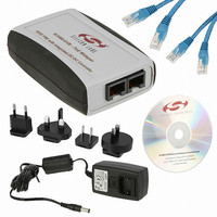
BOARD EVAL POE FOR SI3460
Manufacturer
Silicon Laboratories Inc
Type
DC/DC Switching Converters, Regulators & Controllersr
Specifications of SI3460-EVB
Main Purpose
Special Purpose DC/DC, Power Over Ethernet
Outputs And Type
1, Non-Isolated
Voltage - Output
-48V
Board Type
Fully Populated
Utilized Ic / Part
Si3460
Input Voltage
12 V, 15 V
Output Voltage
- 48 V
Interface Type
Ethernet
Maximum Operating Temperature
+ 85 C
Minimum Operating Temperature
- 40 C
Product
Power Management Modules
For Use With/related Products
Si3460
Lead Free Status / RoHS Status
Lead free / RoHS Compliant
Current - Output
-
Voltage - Input
-
Power - Output
-
Frequency - Switching
-
Regulator Topology
-
Lead Free Status / Rohs Status
Lead free / RoHS Compliant
Other names
336-1842


Si3460
4.3. Operating Mode Sequencing
4.3.1. Detection
After powerup and passing the UVLO threshold voltage of 10 V, the Si3460 enters into the detection state, with
FET M2 off and the dc-dc converter disabled so as to generate no output. Prior to turning on the PSE output FET
M2 and enabling the 250 kHz square wave for the dc-dc converter, a valid detection sequence must take place.
According to the IEEE specifications, the detection process consists of sensing a nominal 25 k signature
resistance in parallel with up to 0.15 µF of capacitance. To eliminate the possibility of false detection events, the
Si3460-EVB reference design performs a robust 3-point detection sequence by varying the voltage across the
sense bridge R1, R2, and R3. The fourth leg of the sense bridge is the load that connects to the drain of M2 and
returns to V
At the beginning of the detection sequence, V
impedance, V
signature resistance is in the RGOOD range of 19 to 26.5 k, the Si3460 proceeds to classification and powerup. If
the PD resistance is not in this range, the detection sequence repeats continuously.
Detection is sequenced approximately every 320 msec and repeats until RGOOD is sensed, indicating a valid PD
has been detected. The STATUS LED (D13) is flashed at the 320 ms rate in synchronization with the detection
process to indicate the PSE is searching for a valid PD.
4.3.2. Classification
After a valid PD is detected, the pass transistor, M2, and the PWM controller are turned on and programmed for an
output voltage of 18 V with a current limit of 75 mA. The current measured during the classification process
determines the class level of the PD. If the class level of the PD is not within the supported level as set by the initial
voltage on the Si3460's STATUS pin (refer to the Operating Mode Configuration section above), an error is
declared and the LED blinks rapidly. This is referred to as classification-based power denial. If the class level is in
the supported range, the Si3460 proceeds to powerup. This is referred to as classification-based power granting.
Classification level is determined according to the current at ISENSE as shown in Table 9.
If the classification level is at a greater power than can be supported based on R28 and R30, an error condition is
reported by flashing the LED at a 10 Hz rate for two seconds before the state machine goes back to the detection
cycle.
4.3.3. Classification-Based Current Limiting
Current limits (I
current limits.
12
6.5mA to 14.5 mA
14.5 mA to 23 mA
ISENSE Current
(Nominal)
< 6.5 mA
> 23 mA
EE
OUT
via D8 and L1.
CUT
is then varied from 4.5 to 7.5 V and then back to 4.5 V for 20 ms at each level. If the PD's
)are set based on the classification voltage on the STATUS pin at powerup. Refer to Table 9 for
Classification
Class 3 or 4
Class 0
Class 1
Class 2
Level
Table 9. Classification Levels
Minimum Power
OUT
15.4 W
15.4 W
Level
is at zero output voltage for 250 ms. With a 10 k source
Rev. 1.1
4 W
7 W
Threshold I
Overload Current
400 mA
180 mA
400 mA
98 mA
CUT
(Max)
Overload Current
Limit I
450 mA
450 mA
450 mA
450 mA
LIM
(Max)
Related parts for SI3460-EVB
Image
Part Number
Description
Manufacturer
Datasheet
Request
R

Part Number:
Description:
IC POWER MANAGEMENT CTLR 11VQFN
Manufacturer:
Silicon Laboratories Inc
Datasheet:

Part Number:
Description:
IC POWER MANAGEMENT CTLR 11VQFN
Manufacturer:
Silicon Laboratories Inc
Datasheet:
Part Number:
Description:
IC POWER MANAGEMENT CTLR 11VQFN
Manufacturer:
Silicon Laboratories Inc
Datasheet:
Part Number:
Description:
IC POWER MANAGEMENT CTLR 11VQFN
Manufacturer:
Silicon Laboratories Inc
Datasheet:

Part Number:
Description:
Hot Swap & Power Distribution IEEE 802.3af PSE w/DC-DC CTRLR
Manufacturer:
Silicon Laboratories Inc
Datasheet:
Part Number:
Description:
SMD/C°/SINGLE-ENDED OUTPUT SILICON OSCILLATOR
Manufacturer:
Silicon Laboratories Inc
Part Number:
Description:
Manufacturer:
Silicon Laboratories Inc
Datasheet:
Part Number:
Description:
N/A N/A/SI4010 AES KEYFOB DEMO WITH LCD RX
Manufacturer:
Silicon Laboratories Inc
Datasheet:
Part Number:
Description:
N/A N/A/SI4010 SIMPLIFIED KEY FOB DEMO WITH LED RX
Manufacturer:
Silicon Laboratories Inc
Datasheet:
Part Number:
Description:
N/A/-40 TO 85 OC/EZLINK MODULE; F930/4432 HIGH BAND (REV E/B1)
Manufacturer:
Silicon Laboratories Inc
Part Number:
Description:
EZLink Module; F930/4432 Low Band (rev e/B1)
Manufacturer:
Silicon Laboratories Inc
Part Number:
Description:
I°/4460 10 DBM RADIO TEST CARD 434 MHZ
Manufacturer:
Silicon Laboratories Inc
Part Number:
Description:
I°/4461 14 DBM RADIO TEST CARD 868 MHZ
Manufacturer:
Silicon Laboratories Inc
Part Number:
Description:
I°/4463 20 DBM RFSWITCH RADIO TEST CARD 460 MHZ
Manufacturer:
Silicon Laboratories Inc