LM22670INVEVAL National Semiconductor, LM22670INVEVAL Datasheet

BOARD EVALUATION FOR LM22670INV

LM22670INVEVAL

Manufacturer Part Number
LM22670INVEVAL
Description
BOARD EVALUATION FOR LM22670INV
Manufacturer
National Semiconductor
Series
SIMPLE SWITCHER®r
Datasheets

Specifications of LM22670INVEVAL

Main Purpose
DC/DC, Step Down
Outputs And Type
1, Non-Isolated
Voltage - Output
-5V
Current - Output
1.5A
Voltage - Input
5 ~ 35V
Regulator Topology
Buck
Frequency - Switching
500kHz
Board Type
Fully Populated
Utilized Ic / Part
LM22670
Lead Free Status / RoHS Status
Not applicable / Not applicable
Power - Output
-
Other names
*LM22670INVEVAL
© 2009 National Semiconductor Corporation
LM22670 Evaluation Board
Inverting Topology and
Application Notes
Introduction
The LM22670 inverting evaluation board is designed to
demonstrate the capabilities of the LM22670 switching regu-
lator in a polarity-inverting topology. The LM22670 inverting
evaluation board schematic shown in Figure 1 is configured
to provide an output of minus 5V (-5V) up to 1.5A load current
with an input voltage range of 6V to 35V. The typical operating
frequency is 500 kHz.
The evaluation board is designed to operate at ambient tem-
peratures up to 50°C. Typical evaluation board performance
and characteristics curves are shown in Figure 5 through Fig-
ure 7. Figure 8 shows the PCB layout.
To aid in the design and evaluation of DC/DC polarity-invert-
ing converter solutions based on the LM22670 switching
regulator, the evaluation board can be re-configured for dif-
ferent output voltages.
The evaluation board is designed to highlight applications
with a small solution size. This implies that there will be a
trade-off between size and the area of heat dissipation avail-
able. If this evaluation board is operated continuously at a full
1.5A load, it will get hot. For more negative output voltages
than the pre-adjusted -5V, the total output power as well as
the total power conversion losses will increase.
Test points are provided to enable easy connection and mon-
itoring of critical signals.
For more information about device function and electrical
characteristics, refer to the LM22670 datasheet. The evalua-
tion board can be reconfigured for a different load current and
output voltage. For design limitations, see the IC Device Rat-
ings section.
The performance of the evaluation board is as follows:
Input Range: 6V to 35V, 12V nominal
Output Voltage: -5V
Output Current Range: 0A to 1.5A
Frequency of Operation: 500 kHz
Board Size: 1.5 X 1.65 inches
Package: PSOP-8
300752
National Semiconductor
Application Note 1888
Frederik Dostal
July 9, 2009
Evaluation Board Startup
Before applying power to the LM22670 polarity-inverting eval-
uation board, all external connections should be verified. The
external power supply input must be turned off and connected
with proper polarity to the VIN and GND posts. A load resistor
or electronic load should be connected between the VOUT
and GND posts as desired. Both the VIN and VOUT connec-
tions should use the closest GND posts respective to VIN or
VOUT. The output voltage can be monitored with a multi-me-
ter or oscilloscope at the VOUT post. Once all connections to
the evaluation board have been verified, input power can be
applied. A load resistor or electronic load does not need to be
connected during startup. If the EN test point is left floating,
the output voltage will ramp up when an input voltage is ap-
plied. Make sure that the external power supply (input voltage
power source) is capable of providing enough current so that
the adjusted output voltage can be obtained. Keep in mind
that the startup current will be greater than the steady state
current.
Principle of Operation
The polarity-inverting converter, shown in Figure 1, uses the
basic principle of energy storage in the inductor, L1, during
on-time and transfers the energy through the diode, D1, to the
output during off-time. When the switch turns on, the diode is
reverse biased and the inductor current will ramp up linearly.
When the switch turns off, the inductor will reverse its polarity
in order to maintain the peak switch current. At that time, the
diode, D1, will be forward biased and the energy stored in the
inductor will be transferred to the load as well as the output
capacitor, C4.
Since the switch node is negative with respect to ground, the
output voltage across the output capacitors (C4 and C5) will
become negative.
This type of polarity-inverting converter can step-up and step-
down the magnitude of the input voltage, which makes this
circuit a buck-boost converter. However, the output voltage is
always negative in reference to ground.
www.national.com

Related parts for LM22670INVEVAL

LM22670INVEVAL Summary of contents

Page 1

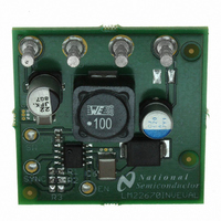
... Input Range 35V, 12V nominal Output Voltage: -5V Output Current Range 1.5A Frequency of Operation: 500 kHz Board Size: 1.5 X 1.65 inches Package: PSOP-8 © 2009 National Semiconductor Corporation National Semiconductor Application Note 1888 Frederik Dostal July 9, 2009 Evaluation Board Startup Before applying power to the LM22670 polarity-inverting eval- uation board, all external connections should be verified ...

Page 2

FIGURE 1. Evaluation Board Schematic Inverting Topology Design Considerations Figure 1 shows the typical configuration of a polarity-inverting converter using the LM22670 switching regulator. This invert- ing topology design can be implemented with any member of the LM2267X SIMPLE SWITCHER ...

Page 3

Inductor Selection Duty-cycle is calculated as: where V is the D1 diode voltage drop and V D drop across the LM22670 internal power N-FET. The R of the FET is specified in the LM22670 datasheet to cal- (ON) culate V ...

Page 4

Input Capacitor Selection The input capacitor needs to be selected based on its low ESR value and the high RMS current rating capable of sup- porting high current changes on the input of the application. Low ESR bypass capacitors located ...

Page 5

... To in- crease the phase margin for applications using low input voltages, select a higher capacitance value for C6 and C7. It TABLE 1. LM22670INVEVAL Bill of Materials for VOUT = -5V, Designed for 1.5A Output Current Ref # C1, C8 2.2 µF 50V ceramic C2 22 µ ...

Page 6

Performance Characteristics Unless otherwise specified 12V FIGURE 5. Start-Up Waveforms (Load Resistor = 4Ω) FIGURE 6. Efficiency vs I www.national.com = 25° -5V. A OUT 30075219 FIGURE 7. Overall Loop Gain and Phase 30075217 ...

Page 7

PCB Layout Diagram 7 30075213 www.national.com ...

Page 8

... FIGURE 8. LM22670INVEVAL PCB Layout 8 30075214 ...

Page 9

9 www.national.com ...

Page 10

... For more National Semiconductor product information and proven design tools, visit the following Web sites at: Products Amplifiers www.national.com/amplifiers Audio www.national.com/audio Clock and Timing www.national.com/timing Data Converters www.national.com/adc Interface www.national.com/interface LVDS www.national.com/lvds Power Management www.national.com/power Switching Regulators www.national.com/switchers LDOs www.national.com/ldo LED Lighting www ...

Related keywords