ADP2114-2PH-EVALZ Analog Devices Inc, ADP2114-2PH-EVALZ Datasheet - Page 32
ADP2114-2PH-EVALZ
Manufacturer Part Number
ADP2114-2PH-EVALZ
Description
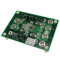
BOARD EVALUATION 1.2V 4A 1.2MHZ
Manufacturer
Analog Devices Inc
Type
Evaluation Boardr
Specifications of ADP2114-2PH-EVALZ
Design Resources
Powering AD9268 with ADP2114 for Increased Efficiency (CN0137)
Main Purpose
DC/DC, Step Down
Outputs And Type
1, Non-Isolated
Voltage - Output
0.6 ~ 3.3 V
Current - Output
4A
Voltage - Input
2.75 ~ 5.5 V
Regulator Topology
Buck
Frequency - Switching
300kHz, 600kHz, 1.2MHz
Board Type
Fully Populated
Utilized Ic / Part
ADP2114
Svhc
No SVHC (18-Jun-2010)
Kit Features
DC-to-DC Switching Regulator, Standalone Capability, Configurable SYNC Input Or CLOCKOUT Output
Mcu Supported Families
ADP2114
Silicon Manufacturer
Analog Devices
Kit Contents
Board
Features
Standalone Capability, Two Independent Enable Inputs, Two Power Good Outputs
Core Architecture
Power
Rohs Compliant
Yes
Kit Application Type
Power Management
Application Sub Type
Step Down DC/DC Regulator
Lead Free Status / RoHS Status
Lead free / RoHS Compliant
Power - Output
-
Lead Free Status / RoHS Status
Lead free / RoHS Compliant, Lead free / RoHS Compliant
Available stocks
Company
Part Number
Manufacturer
Quantity
Price
Company:

Part Number:
ADP2114-2PH-EVALZ
Manufacturer:
Analog Devices Inc
Quantity:
135


ADP2114
5.
Table 11. Channel 2 Circuit Settings
Circuit Parameter
Output Voltage, V
Reference Voltage, V
Error Amp Transconductance, g
Current Sense Gain, C
Switching Frequency, f
Crossover Frequency, f
Zero Frequency, f
Output Inductor, L
Output Capacitors, C
Compensation Resistor, R
Compensation Capacitor, C
Table 12. Selection Table of L, C
f
300
300
300
300
600
600
600
600
1200
1200
1200
1200
SW
(kHz)
Calculate the feedback loop, compensation component
values by using Equation 15.
H(s) = g
In this case, the following values are substituted for the
variables in Equation 18:
g
G
V
V
C
account for dc bias).
From Equation 18,
R
Substituting R
m
OUT
COMP
CS
REF
OUT
= 550 μs
= 4
= 0.6 V
= 0.8 × (47+22) μF (capacitance derated by 20% to
= 1.8 V
= 22 kΩ.
m
× G
V
5
5
5
5
5
5
5
5
5
5
5
5
ZERO
IN
OUT
OUT
CS
COMP
(V)
REF
×
OUT
CS
CROSS
SW
V
V
in Equation 19 yields C
OUT
REF
COMP
COMP
V
3.3
2.5
1.8
1.2
3.3
2.5
1.8
1.2
2.5
1.8
1.2
0.8
OUT
× Z
m
OUT
(V)
COMP
, and Compensation Values
Setting
Nominal
Typical
Typical
Typical
Step 2
1/12 f
1/8 f
Step 3
Step 4
Equation 18
Equation 19
(s) × Z
CROSS
SW
Maximum Load (A)
2.0
2.0
2.0
2.0
2.0
2.0
2.0
2.0
2.0
2.0
2.0
2.0
FILT
(s)
COMP
Value
1.8 V
0.6 V
550 μs
4 A/V
600 kHz
50 kHz
6.25 kHz
3.3 μF
47 μF + 22 μF
22 kΩ
1100 pF
= 1100 pF.
Rev. 0 | Page 32 of 40
L (μH)
6.8
6.8
6.8
4.7
3.3
3.3
3.3
2.2
1.8
1.8
1.2
1.0
SYSTEM CONFIGURATION
Complete the following steps to further configure the ADP2114
for this design example:
1.
2.
3.
A schematic of the ADP2114 as configured in the design example
described in this section is shown in Figure 79.
Table 12 provides the recommended inductor, output capacitor,
and compensation component values for a set of popular input
and output voltage combinations.
Set the switching frequency (f
by connecting the FREQ pin through an 8.2 kΩ resistor
to GND.
Tie SCFG to VDD and use the CLKOUT signal to
synchronize other converters on the same board with the
ADP2114.
Tie OPCFG to GND for 2 A/2 A maximum output current
operation and to enable pulse skip mode at light load
conditions (see Table 7).
C
69 (47 + 22)
100
147 (100 + 47)
200 (2 × 100 )
47
57 (47 + 10)
69 (47 + 22)
100
32 (22 + 10)
44 (2 × 22)
57 (47 + 10)
100
OUT
(μF)
R
20
22
22
20
27
24
22
20
27
27
24
27
COMP
SW
) = 600 kHz (see Table 5)
(kΩ)
C
2400
2400
2400
2400
1000
1100
1100
1200
470
470
510
470
COMP
(pF)
Related parts for ADP2114-2PH-EVALZ
Image
Part Number
Description
Manufacturer
Datasheet
Request
R

Part Number:
Description:
BOARD EVALUATION 3.3V/1.8V
Manufacturer:
Analog Devices Inc
Datasheet:

Part Number:
Description:
Configurable, Dual 2 A/Single 4 A, Synchronous Step-Down DC-to-DC Regulator
Manufacturer:
Analog Devices
Datasheet:

Part Number:
Description:
Blank ADISimPower Eval ADP2114
Manufacturer:
Analog Devices Inc
Datasheet:

Part Number:
Description:
±1.7g Dual-Axis IMEMS Accelerometer Evaluation Board
Manufacturer:
Analog Devices Inc
Datasheet:
Part Number:
Description:
Inertial Sensor Evaluation System
Manufacturer:
Analog Devices Inc
Datasheet:
Part Number:
Description:
Manufacturer:
Analog Devices Inc
Datasheet:
Part Number:
Description:
Manufacturer:
Analog Devices Inc
Datasheet:
Part Number:
Description:
Manufacturer:
Analog Devices Inc
Datasheet:
Part Number:
Description:
Manufacturer:
Analog Devices Inc
Datasheet:
Part Number:
Description:
Manufacturer:
Analog Devices Inc
Datasheet:
Part Number:
Description:
Manufacturer:
Analog Devices Inc
Datasheet:
Part Number:
Description:
Manufacturer:
Analog Devices Inc
Datasheet:
Part Number:
Description:
Manufacturer:
Analog Devices Inc
Datasheet: