DAK-89 Power Integrations, DAK-89 Datasheet - Page 7
DAK-89
Manufacturer Part Number
DAK-89
Description
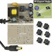
DESIGN ACCELERATOR KIT XT SWITCH
Manufacturer
Power Integrations
Series
LinkSwitch®-XTr
Specifications of DAK-89
Main Purpose
AC/DC, Primary Side
Outputs And Type
1, Isolated
Power - Output
2W
Voltage - Output
6.2V
Current - Output
322mA
Voltage - Input
85 ~ 265VAC
Regulator Topology
Flyback
Board Type
Bare (Unpopulated) and Fully Populated
Utilized Ic / Part
LNK362, LNK363, LNK364
Lead Free Status / RoHS Status
Lead free / RoHS Compliant
Frequency - Switching
-
Lead Free Status / Rohs Status
Lead free / RoHS Compliant
Other names
596-1105


08-Nov-2005
EP-89 6.2 V, 322 mA Adapter
4 Circuit Description
This converter is configured as a flyback. The output voltage is sensed and compared to
a reference (VR1) on the secondary side of the supply, and the results are fed back to U1
(LNK362P) through optocoupler U2 (PC817A). This enables U1 to tightly regulate the
output voltage across the entire load range. Past the point of peak power delivery, U1
will go into auto-restart, and the average power delivered to the load will be limited to
about 5% of full load. This circuit takes advantage of Power Integrations Clampless™
transformer techniques, which use the primary winding capacitance of the transformer to
clamp the voltage spike that is induced on the drain-node, by the transformer leakage
inductance, each time the integrated MOSFET switch within U1 turns off. Therefore, this
converter has no primary clamp components connected to the drain-node.
4.1 Input Filter
Diodes D1 through D4 rectify the AC input. The resulting DC is filtered by bulk storage
capacitors C1 and C2. Inductor L1 and capacitors C1 and C2 form a pi (π) filter that
attenuates differential-mode conducted EMI noise. Resistor R1 dampens the ringing of
the EMI filter. L2 also attenuates conducted EMI noise in the primary return. This
configuration, combined with the LinkSwitch-XT‘s integrated switching frequency jitter
function and Power Integrations E-shield technology used in the construction of the
transformer enable this design to meet EN55022 Class-B conducted EMI requirements
with good margin. An optional 100 pF Y capacitor (C4) can be used to improve the unit-
to-unit repeatability of the EMI measurements. Even with C4 installed, the line frequency
leakage current is less than 10 µA.
4.2 LNK362 Primary
The LNK362P (U1) has the following functions integrated onto a monolithic IC: a 700 V
power MOSFET, a low-voltage CMOS controller, a high-voltage current source (provides
startup and steady-state operational current to the IC), hysteretic thermal shutdown and
auto-restart. The excellent switching characteristics of the integrated power MOSFET
allows efficient operation up to 132 kHz.
The rectified and filtered input voltage is applied to one side of the primary winding of T1.
The other side of the T1 primary winding is connected to the DRAIN pin of U1. As soon
as the voltage across the DRAIN and SOURCE pins of U1 exceeds 50 V, the internal
high voltage current source (connected to the DRAIN pin of the IC) begins charging the
capacitor (C3) connected to the Bypass (BP) pin. Once the voltage across C3 reaches
5.8 V, the controller enables MOSFET switching. MOSFET current is sensed (internally)
by the voltage developed across the DRAIN-to-SOURCE resistance (R
) while it is
DS(ON)
turned on. When the current reaches the preset (internal) current-limit trip point (I
),
LIMIT
the controller turns the MOSFET off. The controller also has a maximum duty cycle
(DC
) signal that will turn the MOSFET off if I
is not reached before the time
MAX
LIMIT
duration equal to maximum duty cycle has elapsed.
Power Integrations
Tel: +1 408 414 9200 Fax: +1 408 414 9201
Page 7 of 32
www.powerint.com
Related parts for DAK-89
Image
Part Number
Description
Manufacturer
Datasheet
Request
R

Part Number:
Description:
KIT DESIGN ACCELERATOR MODEM
Manufacturer:
Power Integrations
Datasheet:

Part Number:
Description:
KIT DESIGN ACCELERATOR SET TOP
Manufacturer:
Power Integrations
Datasheet:

Part Number:
Description:
KIT REF DES DPA 6.6W DC-DC CONV
Manufacturer:
Power Integrations
Datasheet:

Part Number:
Description:
KIT DESIGN ACCELERATOR POE CONV
Manufacturer:
Power Integrations
Datasheet:

Part Number:
Description:
DESIGN ACCELERATOR KIT LP SWITCH
Manufacturer:
Power Integrations
Datasheet:

Part Number:
Description:
KIT DESIGN ACC PEAKSWITCH FAMILY
Manufacturer:
Power Integrations
Datasheet:

Part Number:
Description:
KIT DESIGN ACCELERATOR ADAPTER
Manufacturer:
Power Integrations
Datasheet:

Part Number:
Description:
KIT DESIGN ACCELERATOR ADAPTER
Manufacturer:
Power Integrations
Datasheet:

Part Number:
Description:
KIT DESIGN ACCELERATOR DC-DC
Manufacturer:
Power Integrations
Datasheet:

Part Number:
Description:
KIT DESIGN ACCELERATOR DPA SW
Manufacturer:
Power Integrations
Datasheet: