NCP4894FCEVB ON Semiconductor, NCP4894FCEVB Datasheet - Page 12
NCP4894FCEVB
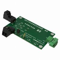
Manufacturer Part Number
NCP4894FCEVB
Description
EVAL BOARD FOR NCP4894FC
Manufacturer
ON Semiconductor
Specifications of NCP4894FCEVB
Design Resources
NCP4894 Demo Board BOM NCP4894FCEVB Gerber Files NCP4894 Demo Board Schematic
Amplifier Type
Class AB
Output Type
1-Channel (Mono)
Max Output Power X Channels @ Load
1.8W x 1 @ 8 Ohm
Voltage - Supply
2.2 V ~ 5.5 V
Board Type
Fully Populated
Utilized Ic / Part
NCP4894
Lead Free Status / RoHS Status
Lead free / RoHS Compliant
Operating Temperature
-
Lead Free Status / Rohs Status
Lead free / RoHS Compliant
For Use With/related Products
NCP4894FC
Other names
NCP4894FCEVBOS


Detailed Description
until 5.5 V power supply. It delivers 320 mW rms output
power to 4.0 W load (VP = 2.6 V) and 1.0 W rms output
power to 8.0 W load (VP = 5.0 V).
two identical internal power amplifiers. Both are externally
configurable with gain−setting resistors R
closed−loop gain is fixed by the ratios of these resistors).
The load is driven differentially through OUTA and OUTB
outputs. This configuration eliminates the need for an
output coupling capacitor.
Internal Power Amplifier
were designed to deliver the output power of the
specifications without clipping. The channel resistance
(R
0.6 W when they drive current.
composed of three symmetrical gain stages, first and
medium gain stages are transconductance gain stages to
obtain maximum bandwidth and DC gain.
Turn−On and Turn−Off Transitions
illustrated with plots that show both single ended signals on
the previous page.
transitions, output power in the load must be slowly
established or cut. When logic high is applied to the
shutdown pin, the bypass voltage begins to rise
exponentially and once the output DC level is around the
common mode voltage, the gain is established slowly
(20 ms). Using this turn−on mode, the device is optimized
in terms of rejection of “pop and click” noises.
the following formula.
by a logic low on the shutdown pin. During the shutdown
mode, amplifier outputs are connected to the ground.
However, to totally cut the output audio signal, you only
need to wait for 20 ms.
Shutdown Function
and SD MODE pins are in the same logic state. This brings
flexibility to the design, as the SD MODE pin must be
permanently connected to VP or GND on the PCB. If the
SD SELECT pin is not connected to the output of a
microcontroller or microprocessor, it’s not advisable to let
it float. A pulldown or pullup resistor is then suitable.
The NCP4894 audio amplifier can operate under 2.6 V
The structure of the NCP4894 is basically composed of
The output PMOS and NMOS transistors of the amplifier
The structure of the internal power amplifier is
A cycle with a turn−on and turn−off transition is
In order to eliminate “pop and click” noises during
A theoretical value of turn−on time at 25°C is given by
C
R: internal 150 k resistor with a 25% accuracy
The device has the same behavior when it is turned−off
The device enters shutdown mode once the SD SELECT
on
by
) of the NMOS and PMOS transistors does not exceed
T
: bypass capacitor
on
= 0.95 * R * C
by
APPLICATION INFORMATION
in
and R
http://onsemi.com
f
(the
NCP4894
12
− The possible output power is four times larger (the
− Output pins (OUTA and OUTB) are biased at the same
During the shutdown state, the DC quiescent current has a
typical value of 10 nA.
Current Limit Circuit
(Porms = 1.0 W, VP = 5.0 V, R
current in the load of 500 mA.
load when a short−circuit occurs between both outputs, the
current limit in the load is fixed to 800 mA.
Thermal Overload Protection
temperature exceeds 160°C, and will be switched on again
only when the temperature decreases below 140°C.
external components besides gain−setting resistors, an
input coupling capacitor and a proper bypassing capacitor
in the typical application.
and R
advantages:
given by
the voltage seen by the load and V
the input differential signal.
output voltage).
output power, check that the amplifier is not current limited
or clipped.
is 500 mA
P orms
The
In order to limit the excessive power dissipation in the
Internal
The NCP4894 is unity−gain stable and requires no
Both internal amplifiers are externally configurable (R
The differential−ended amplifier presents two major
The differential closed loop−gain of the amplifier is
Output power delivered to the load is given by
When choosing gain configuration to obtain the desired
The maximum current which can be delivered to the load
output swing is doubled) as compared to a single−ended
amplifier under the same conditions.
potential VP/2, this eliminates the need for an output
coupling capacitor required with a single−ended
amplifier configuration.
in
+
) with gain configuration.
maximum
A vd
(Vopeak) 2
I opeak
amplifiers are switched off when the
2 * R L
+
*
R in
R f
+
V opeak
+
output
(Vopeak is the peak differential
R L
V inrms
V orms
.
L
power
.
= 8.0 W) requires a peak
V
inrms
orms
is the rms value of
is the rms value of
of
the
circuit
f
Related parts for NCP4894FCEVB
Image
Part Number
Description
Manufacturer
Datasheet
Request
R

Part Number:
Description:
Differential Audio Power Amplifier
Manufacturer:
ON Semiconductor
Datasheet:
Part Number:
Description:
ON Semiconductor [VOLTAGE REGULATOR]
Manufacturer:
ON Semiconductor
Datasheet:
Part Number:
Description:
357-036-542-201 CARDEDGE 36POS DL .156 BLK LOPRO
Manufacturer:
ON Semiconductor
Datasheet:
Part Number:
Description:
357-036-542-201 CARDEDGE 36POS DL .156 BLK LOPRO
Manufacturer:
ON Semiconductor
Datasheet:
Part Number:
Description:
357-036-542-201 CARDEDGE 36POS DL .156 BLK LOPRO
Manufacturer:
ON Semiconductor
Datasheet:
Part Number:
Description:
357-036-542-201 CARDEDGE 36POS DL .156 BLK LOPRO
Manufacturer:
ON Semiconductor
Datasheet:
Part Number:
Description:
357-036-542-201 CARDEDGE 36POS DL .156 BLK LOPRO
Manufacturer:
ON Semiconductor
Datasheet:
Part Number:
Description:
357-036-542-201 CARDEDGE 36POS DL .156 BLK LOPRO
Manufacturer:
ON Semiconductor
Datasheet:
Part Number:
Description:
357-036-542-201 CARDEDGE 36POS DL .156 BLK LOPRO
Manufacturer:
ON Semiconductor
Datasheet:
Part Number:
Description:
357-036-542-201 CARDEDGE 36POS DL .156 BLK LOPRO
Manufacturer:
ON Semiconductor
Datasheet:
Part Number:
Description:
357-036-542-201 CARDEDGE 36POS DL .156 BLK LOPRO
Manufacturer:
ON Semiconductor
Datasheet:
Part Number:
Description:
357-036-542-201 CARDEDGE 36POS DL .156 BLK LOPRO
Manufacturer:
ON Semiconductor
Datasheet:
Part Number:
Description:
Manufacturer:
ON Semiconductor
Datasheet:
Part Number:
Description:
Manufacturer:
ON Semiconductor
Datasheet: