NCP2809AEVB ON Semiconductor, NCP2809AEVB Datasheet - Page 4
NCP2809AEVB
Manufacturer Part Number
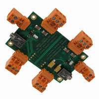
NCP2809AEVB
Description
EVAL BOARD FOR NCP2809A
Manufacturer
ON Semiconductor
Series
NOCAP™r
Specifications of NCP2809AEVB
Design Resources
NCP2809AEVB BOM NCP2809AEVB Gerber Files NCP2809AEVB Schematic
Amplifier Type
Class AB
Output Type
Headphones, 2-Channel (Stereo)
Max Output Power X Channels @ Load
135mW x 2 @ 16 Ohm
Voltage - Supply
2.2 V ~ 5.5 V
Board Type
Fully Populated
Utilized Ic / Part
NCP2809
Lead Free Status / RoHS Status
Lead free / RoHS Compliant
Operating Temperature
-
Lead Free Status / Rohs Status
Lead free / RoHS Compliant
For Use With/related Products
NCP2809A
Other names
NCP2809AEVBOS
Available stocks
Company
Part Number
Manufacturer
Quantity
Price
Company:

Part Number:
NCP2809AEVB
Manufacturer:
ON Semiconductor
Quantity:
2


Stresses exceeding Maximum Ratings may damage the device. Maximum Ratings are stress ratings only. Functional operation above the
Recommended Operating Conditions is not implied. Extended exposure to stresses above the Recommended Operating Conditions may affect
device reliability.
1. Human Body Model, 100 pF discharged through a 1.5 kW resistor following specification JESD22/A114 8.0 kV can be applied on OUT_L,
2. Machine Model, 200 pF discharged through all pins following specification JESD22/A115.
3. Maximum ratings per JEDEC standard JESD78.
*This device contains 752 active transistors and 1740 MOS gates.
PIN FUNCTION DESCRIPTION
MAXIMUM RATINGS
Supply Voltage
Operating Supply Voltage
Input Voltage
Max Output Current
Power Dissipation
Operating Ambient Temperature
Max Junction Temperature
Storage Temperature Range
Thermal Resistance, Junction−to−Air
ESD Protection
Latch up current at Ta = 85_C (Note 3)
Pin
10
OUT_R, REF_I and OUT_I outputs. For other pins, 2.0 kV is the specified voltage.
1
2
3
4
5
6
7
8
9
Type
O
O
O
O
I
I
I
I
I
I
SHUTDOWN
BYPASS
Symbol
OUT_R
OUT_L
OUT_I
REF_I
IN_R
IN_L
(T
V
V
A
P
M
= +25°C)
Rating
Negative input of the second amplifier. It receives the audio input signal. Connected to the input
capicator C
The device enters in shutdown mode when a a low level is applied on this pin.
Bypass capacitor pin which provides the common mode voltage (V
Virtual ground amplifier feed back. This pin sets the stereo headset ground. In order to improve
crosstalk, this pin must be connected as close as possible to the ground connection of the headset
(ideally at the ground pin of the headset connector). When one uses bypassing capacitors, this pin
must be left unconnected.
Negative input of the first amplifier. It receives the audio input signal. Connected to the input
capacitor C
Stereo headset amplifier analog output left. This pin will output the amplified analog signal and,
depending on the application, must be coupled with a capacitor or directly connected to the left
loudspeaker of the headset. This output is able to drive a 16 W load in a single−ended configuration.
Positive analog supply of the cell. Range: 2.2 V – 5.5 V
Virtual ground for stereo Headset common connection. This pin is directly connected to the
common connection of the headset when use of bypassing capacitor is not required. When one
uses bypassing capacitors, this pin must be left unconnected.
Analog Ground
Stereo headset amplifier analog output right. This pin will output the amplified analog signal and,
depending on the application, must be coupled with a capacitor or directly connected to the right
loudspeaker of the headset. This output is able to drive a 16 W load in a single−ended configuration.
Human Body Model (HBM) (Note 1)
Machine Model (MM) (Note 2)
in
in
(NCP2809A) or the external R
(NCP2809A) or the external R
http://onsemi.com
4
Micro10
UDFN
Description
in
in
(NCP2809B).
(NCP2809B).
Symbol
O
R
T
I
V
V
P
T
p
T
out
qJA
stg
−
in
A
p
d
J
V
p
−0.3 to V
Internally Limited
P
/2).
−65 to +150
−40 to +85
2.2 to 5.5
Value
8000
±100
250
150
200
240
200
6.0
CC
+ 0.3
°C/W
Unit
mA
mA
°C
°C
°C
V
V
V
V
−
Related parts for NCP2809AEVB
Image
Part Number
Description
Manufacturer
Datasheet
Request
R

Part Number:
Description:
ON Semiconductor [VOLTAGE REGULATOR]
Manufacturer:
ON Semiconductor
Datasheet:
Part Number:
Description:
357-036-542-201 CARDEDGE 36POS DL .156 BLK LOPRO
Manufacturer:
ON Semiconductor
Datasheet:
Part Number:
Description:
357-036-542-201 CARDEDGE 36POS DL .156 BLK LOPRO
Manufacturer:
ON Semiconductor
Datasheet:
Part Number:
Description:
357-036-542-201 CARDEDGE 36POS DL .156 BLK LOPRO
Manufacturer:
ON Semiconductor
Datasheet:
Part Number:
Description:
357-036-542-201 CARDEDGE 36POS DL .156 BLK LOPRO
Manufacturer:
ON Semiconductor
Datasheet:
Part Number:
Description:
357-036-542-201 CARDEDGE 36POS DL .156 BLK LOPRO
Manufacturer:
ON Semiconductor
Datasheet:
Part Number:
Description:
357-036-542-201 CARDEDGE 36POS DL .156 BLK LOPRO
Manufacturer:
ON Semiconductor
Datasheet:
Part Number:
Description:
357-036-542-201 CARDEDGE 36POS DL .156 BLK LOPRO
Manufacturer:
ON Semiconductor
Datasheet:
Part Number:
Description:
357-036-542-201 CARDEDGE 36POS DL .156 BLK LOPRO
Manufacturer:
ON Semiconductor
Datasheet:
Part Number:
Description:
357-036-542-201 CARDEDGE 36POS DL .156 BLK LOPRO
Manufacturer:
ON Semiconductor
Datasheet:
Part Number:
Description:
357-036-542-201 CARDEDGE 36POS DL .156 BLK LOPRO
Manufacturer:
ON Semiconductor
Datasheet:
Part Number:
Description:
Manufacturer:
ON Semiconductor
Datasheet:
Part Number:
Description:
Manufacturer:
ON Semiconductor
Datasheet:
Part Number:
Description:
Manufacturer:
ON Semiconductor
Datasheet: