NCP2990FCT2GEVB ON Semiconductor, NCP2990FCT2GEVB Datasheet

EVAL BOARD FOR NCP2990FCT2G

NCP2990FCT2GEVB

Manufacturer Part Number
NCP2990FCT2GEVB
Description
EVAL BOARD FOR NCP2990FCT2G
Manufacturer
ON Semiconductor
Datasheets

Specifications of NCP2990FCT2GEVB

Design Resources
NCP2990 EVB BOM NCP2990FCT2GEVB Gerber Files NCP2990 EVB Schematic
Amplifier Type
Class AB
Output Type
1-Channel (Mono)
Max Output Power X Channels @ Load
1.35W x 1 @ 8 Ohm
Voltage - Supply
2.2 V ~ 5.5 V
Operating Temperature
-10°C ~ 75°C
Board Type
Fully Populated
Utilized Ic / Part
NCP2990
Lead Free Status / RoHS Status
Lead free / RoHS Compliant
For Use With/related Products
NCP2990FCT2G
Other names
NCP2990FCT2GEVBOS
NCP2990
1.3 Watt Audio Power
Amplifier with Fast Turn On
Time
communication device applications such as mobile phone
applications. The NCP2990 is capable of delivering 1.3 W of
continuous average power to an 8.0 W BTL load from a 5.0 V power
supply, and 1.0 W to a 4.0 W BTL load from a 3.6 V power supply.
external components and minimal power consumption. It features a
low−power consumption shutdown mode, which is achieved by
driving the SHUTDOWN pin with logic low.
noise that would otherwise occur during turn−on and turn−off
transitions. It is a zero pop noise device when a single ended audio
input is used.
controlled gain (with resistors), as well as an externally controlled
turn−on time (with the bypass capacitor). When using a 1 mF bypass
capacitor, it offers 60 ms wake up time.
battery, saving the use of an LDO.
Features
Typical Applications
*For additional information on our Pb−Free strategy and soldering details, please
© Semiconductor Components Industries, LLC, 2007
January, 2007 − Rev.1
download the ON Semiconductor Soldering and Mounting Techniques Reference
Manual, SOLDERRM/D.
The NCP2990 is an audio power amplifier designed for portable
The NCP2990 provides high quality audio while requiring few
The NCP2990 contains circuitry to prevent from “pop and click”
For maximum flexibility, the NCP2990 provides an externally
Due to its superior PSRR, it can be directly connected to the
This device is available in a 9−Pin Flip−Chip CSP (Lead−Free).
60 ms (1 mF Bypass Capacitor)
1.3 W to an 8.0 W BTL Load from a 5.0 V Power Supply
Superior PSRR: Direct Connection to the Battery
Zero Pop Noise Signature with a Single Ended Audio Input
Ultra Low Current Shutdown Mode: 10 nA
2.2 V−5.5 V Operation
External Gain Configuration Capability
External Turn−on Time Configuration Capability:
Up to 1.0 nF Capacitive Load Driving Capability
Thermal Overload Protection Circuitry
This is a Pb−Free Device*
Portable Electronic Devices
PDAs
Wireless Phones
1
See detailed ordering and shipping information in the package
dimensions section on page 12 of this data sheet.
1
ORDERING INFORMATION
MBA
A
Y
WW
G
BYPASS
9−Pin Flip−Chip CSP
VM_P
INM
PIN CONNECTIONS
B1
A1
C1
9−Pin Flip−Chip CSP
http://onsemi.com
CASE 499E
FC SUFFIX
= Specific Device Code
= Assembly Location
= Year
= Work Week
= Pb−Free Package
(Top View)
OUTA
OUTB SHUTDOWN
VM
A2
C2
B2
Publication Order Number:
INP
A3
B3
C3
V
A3
p
DIAGRAMS
MARKING
A1
NCP2990/D
AYWW
MBAG
C1

Related parts for NCP2990FCT2GEVB

NCP2990FCT2GEVB Summary of contents

Page 1

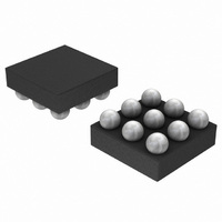
... PDAs • Wireless Phones *For additional information on our Pb−Free strategy and soldering details, please download the ON Semiconductor Soldering and Mounting Techniques Reference Manual, SOLDERRM/D. © Semiconductor Components Industries, LLC, 2007 January, 2007 − Rev.1 http://onsemi.com 9−Pin Flip−Chip CSP ...

Page 2

Ci Ri INM AUDIO INPUT INP BYPASS bypass SHUTDOWN VIH VIL Figure 1. Typical Audio Amplifier Application Circuit with Single Ended Input NCP2990 ...

Page 3

PIN DESCRIPTION Pin Type Symbol A1 I INM A2 O OUTA A3 I INP B1 I VM_P BYPASS C2 O OUTB C3 I SHUTDOWN MAXIMUM RATINGS (Note 1) Rating Supply Voltage ...

Page 4

ELECTRICAL CHARACTERISTICS Limits apply for T Characteristic Supply Quiescent Current Common Mode Voltage Shutdown Current Shutdown Voltage High Shutdown Voltage Low Turning On Time (Note 8) Turning Off Time Output Impedance in Shutdown Mode Output Swing Rms Output Power Maximum ...

Page 5

TYPICAL PERFORMANCE CHARACTERISTICS 2 kHz 1 0.1 0. 100 150 200 P (mW) OUT Figure 2. THD+N versus Output Power 3.6 V ...

Page 6

TYPICAL PERFORMANCE CHARACTERISTICS 1600 = 1400 kHz 1200 THD+N = 10% 1000 800 600 400 200 2.5 3 3.5 4 POWER SUPPLY (V) Figure 8. Output Power versus Power Supply ...

Page 7

TYPICAL PERFORMANCE CHARACTERISTICS − 3 Input to GND A −50 −60 −70 −80 10 100 FREQUENCY (Hz) Figure 14. P versus Frequency and SRR Gain @ ...

Page 8

TYPICAL PERFORMANCE CHARACTERISTICS 0.7 0.6 0 kHz 0.2 THD + N < 0.1% 0 0.2 0.4 0.6 0 OUTPUT POWER (W) ...

Page 9

Detailed Description The NCP2990 audio amplifier can operate under 2.6 V until 5.5 V power supply. With less than 1% THD + N, it can deliver up to 1.2 W RMS output power to an 8.0 W load (V = ...

Page 10

Gain−Setting Resistor Selection ( and R set the closed−loop gain of the amplifier order to optimize device and system performance, the NCP2990 should be used in low gain configurations. The low gain configuration minimizes THD ...

Page 11

Figure 26. Demonstration Board for 9−Pin Flip−Chip CSP Device − Silkscreen Layers http://onsemi.com NCP2990 11 ...

Page 12

... C2, TP1, − TP2, TP3 Marking Package MBA 9−Pin Flip−Chip CSP (Pb−Free) http://onsemi.com 12 Manufacturer Refer- ence Manufacturer ON Semiconductor NCP2990 Panasonic ERJ−6GEYJ203V Panasonic ERJ−6GEYJ203V TDK C2012X7R2A473K TDK C2012X7R1A105K Tyco Electronics / AMP 5−826629−0 Phoenix Contact 1757242 Harwin D3082− ...

Page 13

... SCILLC is an Equal Opportunity/Affirmative Action Employer. This literature is subject to all applicable copyright laws and is not for resale in any manner. PUBLICATION ORDERING INFORMATION LITERATURE FULFILLMENT: Literature Distribution Center for ON Semiconductor P.O. Box 5163, Denver, Colorado 80217 USA Phone: 303−675−2175 or 800−344−3860 Toll Free USA/Canada Fax: 303− ...

Related keywords