CDB35L00 Cirrus Logic Inc, CDB35L00 Datasheet - Page 5
CDB35L00
Manufacturer Part Number
CDB35L00
Description
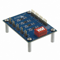
DEVELOPMENT BOARD FOR CS35L0X
Manufacturer
Cirrus Logic Inc
Datasheet
1.CDB35L00.pdf
(12 pages)
Specifications of CDB35L00
Amplifier Type
Class D
Output Type
4-Channel (Quad)
Max Output Power X Channels @ Load
2.7W x 4 @ 4 Ohm
Voltage - Supply
2.5 V ~ 5.5 V
Board Type
Fully Populated
Utilized Ic / Part
CS35L0X
Description/function
Audio Amplifiers
Operating Supply Voltage
2.5 V to 5.5 V
Output Power
1.6 W, 2.7 W
Product
Audio Modules
For Use With/related Products
CS35L00
Lead Free Status / RoHS Status
Contains lead / RoHS non-compliant
Operating Temperature
-
Lead Free Status / Rohs Status
Lead free / RoHS Compliant
Other names
598-1803


DS913DB2
1.4.1
1.5
1.5.1
Gain Control
The amplifier gain of the CS35L00 can be configured to operate with either a +6 dB gain or a +12 dB gain
as shown in
This is connected to the GAIN_SEL pins on the four CS35L00 devices as shown in
Note:
Shutdown Control Resistors
The CDB35L00-X4 contains 0 ohm resistors (R1-R4) which
allow the individual CS35L00 shutdown pins to be discon-
nected from the S1 switch or connected to an external con-
trol device. These resistors are located on the back side of
the CDB35L00-X4 board near S1, as shown highlighted in
blue in
R1-R4 are connected to SD on U1-U4, respectively. It is rec-
ommended that the individual shutdown line pull-up resistors
for U1-U4 (R10, R20, R30, R40) be left populated to help
prevent the individual SD control lines from floating.
Optional Gain Adjustment Resistors
The CDB35L00-X4 contains optional gain adjustment resistor placeholders for each CS35L00 device
(R11, R12, R21, R22, R31, R32, R41, R42). By default these are not populated and the CS35L00 oper-
ates at its gain control setting as set by the S1 switch. See
necessary when a gain of +6 dB or a gain of +12 dB is not desired. By adding series resistance to the
input, the signal amplitude to the CS35L00 will be reduced, and will reduce the overall system gain. The
typical input impedance values of the CS35L00 as well as how to calculate the resistor values for a de-
sired gain can be found in the device datasheet.
In order to use the optional gain adjustment resistors for U1, the traces between the R11 pads and the
traces between the R12 pads must be cut in order to break the bypass circuit before populating R11 and
R12 with the desired resistance values. The location of these required cuts are shown in
6. After the trace between the pads has been broken, the gain adjustment resistors can be added to the
board.
The gain adjustment resistors for U2, U3, and U4 can be added in the same manner as is described for
U1 (above).
The CS35L00 devices should be placed into shutdown via either the S1 switch or by removing pow-
er before changing the GAIN setting.
Figure
Table 1 on page
2.
Table 3. S1 Switch Default Shutdown Configurations
HIGH
LOW
3. The amplifier gain is selectable through the GAIN setting on the S1 switch.
U1 & U2 OFF
U1 & U2 ON
SD1-2
U3 & U4 OFF
U3 & U4 ON
Table
SD3-4
Figure 2. Shutdown Control Resistors
1. The gain adjustment resistors are only
Figure 4 on page
CDB35L00-X4
Figure 3 on page
9.
5
Related parts for CDB35L00
Image
Part Number
Description
Manufacturer
Datasheet
Request
R

Part Number:
Description:
Audio Modules & Development Tools Eval Bd - DF 4ch ADC 8ch DAC & 32bit DSP
Manufacturer:
Cirrus Logic Inc
Part Number:
Description:
Development Kit
Manufacturer:
Cirrus Logic Inc
Datasheet:
Part Number:
Description:
Development Kit
Manufacturer:
Cirrus Logic Inc
Datasheet:


Part Number:
Description:
High-efficiency PFC + Fluorescent Lamp Driver Reference Design
Manufacturer:
Cirrus Logic Inc
Datasheet:
Part Number:
Description:
Development Kit
Manufacturer:
Cirrus Logic Inc
Datasheet:
Part Number:
Description:
Development Kit
Manufacturer:
Cirrus Logic Inc
Datasheet:

Part Number:
Description:
Development Kit
Manufacturer:
Cirrus Logic Inc
Datasheet:
Part Number:
Description:
Development Kit
Manufacturer:
Cirrus Logic Inc
Datasheet:
Part Number:
Description:
Development Kit
Manufacturer:
Cirrus Logic Inc
Datasheet:

Part Number:
Description:
EVALUATION BOARD FOR CS8427
Manufacturer:
Cirrus Logic Inc
Datasheet:

Part Number:
Description:
BOARD EVAL FOR CS8416 RCVR
Manufacturer:
Cirrus Logic Inc
Datasheet:

Part Number:
Description:
EVALUATION BOARD FOR CS8420
Manufacturer:
Cirrus Logic Inc
Datasheet:

Part Number:
Description:
KIT DEVELOPMENT EP9315 ARM9
Manufacturer:
Cirrus Logic Inc
Datasheet:

Part Number:
Description:
KIT DEVELOPMENT EP9302 ARM9
Manufacturer:
Cirrus Logic Inc
Datasheet: