ADC101C02XEB/NOPB National Semiconductor, ADC101C02XEB/NOPB Datasheet - Page 4
ADC101C02XEB/NOPB
Manufacturer Part Number
ADC101C02XEB/NOPB
Description
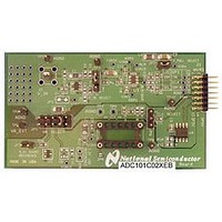
BOARD EVALUATION FOR ADC101C02X
Manufacturer
National Semiconductor
Specifications of ADC101C02XEB/NOPB
Number Of Adc's
1
Number Of Bits
10
Sampling Rate (per Second)
188.9k
Data Interface
I²C
Inputs Per Adc
1 Single Ended
Power (typ) @ Conditions
780mW @ 22kSPS
Voltage Supply Source
Single Supply
Operating Temperature
-40°C ~ 105°C
Utilized Ic / Part
ADC101C021, ADC101C027
Silicon Manufacturer
National
Silicon Core Number
ADC101C021, ADC101C027
Kit Application Type
Data Converter
Application Sub Type
ADC
Kit Contents
Board
Lead Free Status / RoHS Status
Lead free / RoHS Compliant
Other names
ADC101C02XEB


www.national.com
STATIC CONVERTER CHARACTERISTICS
DYNAMIC CONVERTER CHARACTERISTICS
Symbol
SINAD
Absolute Maximum Ratings
(Notes 1, 2)
If Military/Aerospace specified devices are required,
please contact the National Semiconductor Sales Office/
Distributors for availability and specifications.
Electrical Characteristics
The following specifications apply for V
f
unless otherwise noted.
ENOB
IN
V
SNR
DNL
THD
Supply Voltage, V
Voltage on any Analog Input Pin to
GND
Voltage on any Digital Input Pin to
GND
Input Current at Any Pin (Note 3)
Package Input Current (Note 3)
Power Dissipation at T
ESD Susceptibility (Note 5)
Junction Temperature
Storage Temperature
INL
GE
OFF
= 10kHz for f
(CDM)
V
ADR pins:
SDA, SCL pins:
A
Human Body Model
Machine Model
Charged Device Model
Human Body Model
Machine Model
, GND, V
Resolution with No Missing Codes
Integral Non-Linearity (End Point
Method)
Differential Non-Linearity
Offset Error
Gain Error
Effective Number of Bits
Signal-to-Noise Ratio
Total Harmonic Distortion
Signal-to-Noise Plus Distortion Ratio
SCL
IN
, ALERT,
A
= 3.4MHz unless otherwise noted. Boldface limits apply for T
Parameter
A
= 25°C
A
−0.3V to (V
= +2.7V to +5.5V, GND = 0V, f
−65°C to +150°C
-0.3V to +6.5V
−0.3V to 6.5V
See (Note 4)
V
V
(Note 13)
V
V
(Note 13)
V
f
V
(Note 13)
V
V
V
V
V
V
V
V
SCL
A
A
A
A
A
A
A
A
A
A
A
A
A
A
A
= +2.7V to +3.6V
= +2.7V to +5.5V. f
= +2.7V to +3.6V
= +2.7V to +5.5V. f
= +2.7V to +3.6V
= +2.7V to +5.5V. f
= +2.7V to +3.6V
= +3.6V to +5.5V
= +2.7V to +3.6V
= +3.6V to +5.5V
= +2.7V to +3.6V
= +3.6V to +5.5V
= +2.7V to +3.6V
= +3.6V to +5.5V
±15 mA
±20 mA
+150°C
up to 3.4 MHz
+0.3V)
2500V
1250V
8000V
250V
400V
Conditions
4
Operating Ratings
Package Thermal Resistances
Soldering
Semiconductor's Reflow Temperature Profile specifications.
Refer to www.national.com/packaging. (Note 6)
Operating Temperature Range
Supply Voltage, V
Analog Input Voltage, V
Digital Input Voltage (Note 7)
Sample Rate
SCL
SCL
SCL
SCL
up to 400 kHz
up to 400 kHz
up to 400kHz
up to 3.4MHz, f
8-Lead MSOP
6-Lead TSOT
Package
process
A
= T
A
MIN
IN
(Note 9)
Typical
to T
+0.21
−0.16
+0.25
−0.16
+0.25
+0.27
−88.9
−85.7
-0.13
±0.1
±0.1
IN
= 1kHz for f
9.97
9.94
61.8
61.6
61.8
61.6
must
MAX
: all other limits T
(Notes 1, 2)
comply
(Note 9)
SCL
Limits
−40°C
±0.5
±0.5
+0.7
−0.7
+0.7
−0.7
±0.8
±0.8
9.87
61.2
61.2
−74
10
±1
up to 400kHz,
250°C/W
200°C/W
up to 188.9 ksps
θ
≤
JA
with
+2.7V to 5.5V
T
A
Units (Limits)
A
0V to 5.5V
≤
LSB (max)
LSB (max)
LSB (max)
LSB (max)
LSB (max)
LSB (max)
LSB (max)
= 25°C
LSB (min)
LSB (min)
Bits (min)
dB (max)
0V to V
dB (min)
dB (min)
+105°C
National
Bits
Bits
dB
dB
dB
A
Related parts for ADC101C02XEB/NOPB
Image
Part Number
Description
Manufacturer
Datasheet
Request
R

Part Number:
Description:
National Semiconductor [8-Bit D/A Converter]
Manufacturer:
National Semiconductor
Datasheet:
Part Number:
Description:
National Semiconductor [Media Coprocessor]
Manufacturer:
National Semiconductor
Datasheet:
Part Number:
Description:
Digitally Controlled Tone and Volume Circuit with Stereo Audio Power Amplifier, Microphone Preamp Stage and National 3D Sound
Manufacturer:
National Semiconductor
Datasheet:
Part Number:
Description:
Digitally Controlled Tone and Volume Circuit with Stereo Audio Power Amplifier, Microphone Preamp Stage and National 3D Sound
Manufacturer:
National Semiconductor
Datasheet:
Part Number:
Description:
AC97 Rev 2 Codec with Sample Rate Conversion and National 3D Sound
Manufacturer:
National Semiconductor
Part Number:
Description:
Manufacturer:
National Semiconductor
Datasheet:
Part Number:
Description:
Manufacturer:
National Semiconductor
Datasheet:
Part Number:
Description:
General Purpose, Low Voltage, Low Power, Rail-to-Rail Output Operational Amplifiers
Manufacturer:
National Semiconductor
Datasheet:
Part Number:
Description:
8-bit 20 MSPS flash A/D converter.
Manufacturer:
National Semiconductor
Datasheet:
Part Number:
Description:
Low Noise Quad Operational Amplifier
Manufacturer:
National Semiconductor
Datasheet:
Part Number:
Description:
Quad Differential Line Receivers
Manufacturer:
National Semiconductor
Datasheet:
Part Number:
Description:
Quad High Speed Trapezoidal? Bus Transceiver
Manufacturer:
National Semiconductor
Datasheet:
Part Number:
Description:
Dual Line Receiver
Manufacturer:
National Semiconductor
Datasheet:
Part Number:
Description:
TTL to 10k ECL Level Translator with Latch
Manufacturer:
National Semiconductor
Datasheet: