AD9262-10EBZ Analog Devices Inc, AD9262-10EBZ Datasheet - Page 8
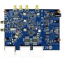
AD9262-10EBZ
Manufacturer Part Number
AD9262-10EBZ
Description
BOARD EVALUATION 10MHZ AD9262
Manufacturer
Analog Devices Inc
Specifications of AD9262-10EBZ
Design Resources
Interfacing ADL5382 to AD9262 as an RF-to-Bits Solution (CN0062)
Number Of Adc's
2
Number Of Bits
16
Sampling Rate (per Second)
160M
Data Interface
Serial, SPI™
Inputs Per Adc
1 Differential
Input Range
2 Vpp
Power (typ) @ Conditions
600mW @ 40MSPS
Voltage Supply Source
Analog and Digital
Operating Temperature
-40°C ~ 85°C
Utilized Ic / Part
AD9262
Silicon Manufacturer
Analog Devices
Application Sub Type
ADC
Kit Application Type
Data Converter
Silicon Core Number
AD9262
Kit Contents
Software, Evaluation Board
Lead Free Status / RoHS Status
Lead free / RoHS Compliant


AD9262
ABSOLUTE MAXIMUM RATINGS
Table 6.
Parameter
Electrical
Environmental
Stresses above those listed under Absolute Maximum Ratings
may cause permanent damage to the device. This is a stress
rating only; functional operation of the device at these or any
other conditions above those indicated in the operational
section of this specification is not implied. Exposure to absolute
maximum rating conditions for extended periods may affect
device reliability.
AVDD to AGND
DVDD to DGND
DRVDD to DGND
AGND to DGND
AVDD to DRVDD
CVDD to CGND
CGND to DGND
D0A to D15A to DGND
D0B to D15B to DGND
DCO to DGND
ORA, ORB to DGND
SDIO to DGND
CSB to AGND
SCLK to AGND
VIN+A/VIN−A, VIN+B/VIN−B to AGND
CLK+, CLK− to CGND
Storage Temperature Range
Operating Temperature Range
Lead Temperature (Soldering, 10 Sec)
Junction Temperature
Rating
−0.3 V to +2.0 V
−0.3 V to +0.3 V
−0.3 V to +2.0 V
−0.3 V to +0.3 V
−0.3 V to +3.9 V
−40°C to +85°C
−0.3 V to +2.0 V
−0.3 V to +3.9 V
−3.9 V to +2.0 V
−0.3 V to +2.0 V
−0.3 V to +2.0 V
−0.3 V to +2.0 V
−0.3 V to +2.0 V
−0.3 V to +3.9 V
−0.3 V to +3.9 V
−0.3 V to +2.5 V
−0.3 V to +2.0 V
−65°C to +125°C
300°C
150°C
Rev. A | Page 8 of 32
THERMAL RESISTANCE
The exposed paddle must be soldered to the ground plane for
the LFCSP package. Soldering the exposed paddle to the PCB
increases the reliability of the solder joints, maximizing the
thermal capability of the package.
Table 7. Thermal Resistance
Package Type
64-Lead LFCSP (CP-64-4)
Typical θ
Airflow increases heat dissipation, effectively reducing θ
addition, metal in direct contact with the package leads from
metal traces, through holes, ground, and power planes reduces
the θ
ESD CAUTION
JA
.
JA
and θ
JC
are specified for a 4-layer board in still air.
θ
21.2
JA
θ
1.1
JC
Unit
°C/W
JA
. In
Related parts for AD9262-10EBZ
Image
Part Number
Description
Manufacturer
Datasheet
Request
R

Part Number:
Description:
BOARD EVALUATION 5MHZ AD9262
Manufacturer:
Analog Devices Inc
Datasheet:
Part Number:
Description:
BOARD EVALUATION FOR AD9262
Manufacturer:
Analog Devices Inc
Datasheet:

Part Number:
Description:
±1.7g Dual-Axis IMEMS Accelerometer Evaluation Board
Manufacturer:
Analog Devices Inc
Datasheet:

Part Number:
Description:
Inertial Sensor Evaluation System
Manufacturer:
Analog Devices Inc
Datasheet:
Part Number:
Description:
Manufacturer:
Analog Devices Inc
Datasheet:
Part Number:
Description:
Manufacturer:
Analog Devices Inc
Datasheet:
Part Number:
Description:
Manufacturer:
Analog Devices Inc
Datasheet:
Part Number:
Description:
Manufacturer:
Analog Devices Inc
Datasheet:
Part Number:
Description:
Manufacturer:
Analog Devices Inc
Datasheet:
Part Number:
Description:
Manufacturer:
Analog Devices Inc
Datasheet:
Part Number:
Description:
Manufacturer:
Analog Devices Inc
Datasheet:
Part Number:
Description:
Manufacturer:
Analog Devices Inc
Datasheet:
Part Number:
Description:
Manufacturer:
Analog Devices Inc
Datasheet: