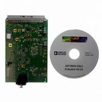
EVAL-AD7766-1EDZ Analog Devices Inc, EVAL-AD7766-1EDZ Datasheet - Page 22

EVAL-AD7766-1EDZ
Manufacturer Part Number
EVAL-AD7766-1EDZ
Description
BOARD EVAL AD7766-1 64KSPS 111DB
Manufacturer
Analog Devices Inc
Specifications of EVAL-AD7766-1EDZ
Number Of Adc's
1
Number Of Bits
24
Sampling Rate (per Second)
64k
Data Interface
Serial
Inputs Per Adc
1 Differential
Input Range
±VREF
Power (typ) @ Conditions
10.5mW @ 64kSPS
Voltage Supply Source
Analog and Digital
Operating Temperature
-40°C ~ 105°C
Utilized Ic / Part
AD7766-1
Lead Free Status / RoHS Status
Lead free / RoHS Compliant
AD7766
V
The AD7766/AD7766-1/AD7766-2 V
voltage in the range of 2.4 V to 2 × AV
recommended that the V
voltage reference. Examples of such references are the ADR445,
ADR435,
Typical reference supply circuits are shown in Figure 46.
The reference voltage input pin (V
supply to the AD7766/AD7766-1/AD7766-2 devices. For a 5 V
V
be applied while voltage supplies to pins AV
This configuration reduces the number of different supplies
required.
The output of the low noise voltage reference does not require a
buffer; however, decoupling the output of the low noise reference is
important. Place a 0.1 μF capacitor at the output of the voltage
reference devices (ADR445, ADR435, ADR425, and ADR421)
and follow the decoupling advice provided for the reference
device chosen.
As mentioned, the nominal supply to the V
achieve the full dynamic range available. When a 2.5 V V
input is used (that is, in low power applications), the signal-to-
noise ratio and dynamic range figures (generated using a 5 V
V
6 dB, a direct result of halving the available input range.
The AD7766/AD7766-1/AD7766-2 devices require a 100 μF
capacitor to ground, which acts as a decoupling capacitor and as
a reservoir of charge for the V
close to the AD7766/AD7766-1/AD7766-2 devices as possible.
Reducing the value of this capacitor (C40 in Figure 46) to 10 μF
typically degrades noise performance by 1 dB. C40 can be an
electrolytic or tantalum capacitor.
REFERENCE
REF+
REF+
SUPPLY
10µF
REF+
C34
Figure 46. AD7766/AD7766-1/AD7766-2 Reference Input Configuration
V+
input, a full-scale input of 5 V on both V
input) quoted in the Specifications section decrease by
INPUT SIGNAL
ADR425
C35
0.1µF
V
IN
(5 V output), and
ADR4xx
REF+
V
OUT
input be generated by a low noise
REF+
0.1µF
C39
pin. Place this capacitor as
REF+
ADR421
) also acts as a power
REF +
DD
(nominally 5 V). It is
C40
100µF
pin is supplied with a
REF+
DD
V
(2.5 V output).
IN+
remain at 2.5 V.
REF+
pin is 5 V to
and V
AD7766-1/
AD7766-2
AD7766/
IN−
REF+
can
Rev. C | Page 22 of 24
MULTIPLEXING ANALOG INPUT CHANNELS
The AD7766/AD7766-1/AD7766-2 can be used with a multi-
plexer configuration. As per any converter that uses a digital
filtering block, the maximum switching rate or the output data
rate per channel is a function of the digital filter settling time.
A user multiplexing the analog inputs to a converter that
employs a digital filter must wait the full digital filter settling
time before a valid conversion result can be achieved; after this
settling time, the channel can be switched. Then, the full
settling time must again be observed before a valid conversion
result is available and the input is switched once more.
The AD7766 filter settling time equals 74 divided by the output
data rate in use. The maximum switching frequency in a multi-
plexed application is, therefore, 1/(74/ODR), where the output
data rate (ODR) is a function of the applied MCLK frequency
and the decimation rate employed by the device in question. For
example, applying a 1.024 MHz MCLK frequency to the AD7766
results in a maximum output data rate of 128 kHz, which in
turn allows a 1.729 kHz multiplexer switching rate.
The AD7766-1 and the AD7766-2 employ digital filters with
longer settling time to achieve greater precision; thus, the
maximum switching frequency for these devices is 864 Hz and
432 Hz, respectively.


