MCP3901EV-MCU16 Microchip Technology, MCP3901EV-MCU16 Datasheet - Page 16
MCP3901EV-MCU16
Manufacturer Part Number
MCP3901EV-MCU16
Description
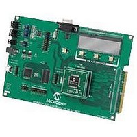
BOARD EVAL FOR 2CH ADC MCP3901
Manufacturer
Microchip Technology
Datasheets
1.MCP3901A0-ISS.pdf
(60 pages)
2.MCP3901A0-ISS.pdf
(30 pages)
3.MCP3901EV-MCU16.pdf
(38 pages)
4.MCP3901EV-MCU16.pdf
(38 pages)
Specifications of MCP3901EV-MCU16
Number Of Adc's
2
Number Of Bits
24
Data Interface
SPI™
Inputs Per Adc
1 Differential
Input Range
±1 V
Voltage Supply Source
Analog and Digital
Operating Temperature
-40°C ~ 85°C
Utilized Ic / Part
MCP3901
Silicon Manufacturer
Microchip
Application Sub Type
ADC
Kit Application Type
Data Converter
Silicon Core Number
MCP3901, PIC24F, PIC24H, DsPIC33, PIC18F86J55
Kit Contents
Board
Lead Free Status / RoHS Status
Lead free / RoHS Compliant


MCP3901
3.4
CH0- and CH0+, and CH1- and CH1+, are the two fully
differential analog voltage inputs for the Delta-Sigma
ADCs.
The linear and specified region of the channels are
dependent on the PGA gain. This region corresponds
to a differential voltage range of ±500 mV/GAIN with
V
The maximum absolute voltage, with respect to AGND,
for each CHn+/- input pin is ±1V with no distortion and
±6V with no breaking after continuous voltage.
3.5
AGND is the ground connection to internal analog
circuitry (ADCs, PGA, voltage reference, POR). To
ensure accuracy and noise cancellation, this pin must
be connected to the same ground as DGND, preferably
with a star connection. If an analog ground plane is
available, it is recommended that this pin be tied to this
plane of the PCB. This plane should also reference all
other analog circuitry in the system.
3.6
This pin is the non-inverting side of the differential
voltage reference input for both ADCs or the internal
voltage reference output.
When VREFEXT = 1, and an external voltage
reference source can be used, the internal voltage ref-
erence is disabled. When using an external differential
voltage reference, it should be connected to its V
pin. When using an external single-ended reference, it
should be connected to this pin.
When VREFEXT = 0, the internal voltage reference is
enabled and connected to this pin through a switch.
This voltage reference has minimal drive capability, and
thus, needs proper buffering and bypass capacitances
(10 µF tantalum in parallel with 0.1 µF ceramic) if used
as a voltage source.
For optimal performance, bypass capacitances should
be connected between this pin and AGND at all times,
even when the internal voltage reference is used.
However, these capacitors are not mandatory to
ensure proper operation.
DS22192C-page 16
REF
= 2.4V.
ADC Differential Analog inputs
(CHn+/CHn-)
Analog Ground (AGND)
Non-Inverting Reference Input,
Internal Reference Output
(REFIN+/OUT)
REF
+
reference all other digital circuitry in the system.
3.7
This pin is the inverting side of the differential voltage
reference input for both ADCs. When using an external
differential voltage reference, it should be connected to
its V
voltage reference, or when VREFEXT = 0 (default) and
using the internal voltage reference, this pin should be
directly connected to AGND.
3.8
DGND is the ground connection to internal digital
circuitry (SINC filters, oscillator, serial interface). To
ensure accuracy and noise cancellation, DGND must be
connected to the same ground as AGND, preferably with
a star connection. If a digital ground plane is available, it
is recommended that this pin be tied to this plane of the
Printed Circuit Board (PCB). This plane should also
3.9
MDAT0 and MDAT1 are the output pins for the
modulator serial bitstreams of ADC Channels 0 and 1,
respectively. These pins are high-impedance by
default. When the MODOUT<1:0> are enabled, the
modulator bitstream of the corresponding channel is
present on the pin and updated at the AMCLK
frequency. (See
Block”
outputs.) These pins can be directly connected to a
MCU or DSP when a specific digital filtering is needed.
3.10
The data ready pin indicates if a new conversion result
is ready to be read. The default state of this pin is high
when DR_HIZN = 1 and is high-impedance when
DR_HIZN = 0 (default). After each conversion is
finished, a low pulse will take place on the data ready
pin to indicate the conversion result is ready as an
interrupt. This pulse is synchronous with the master
clock and has a defined and constant width.
The data ready pin is independent of the SPI interface
and acts like an interrupt output. The data ready pin state
is not latched and the pulse width (and period) are both
determined by the MCLK frequency, over-sampling rate
and internal clock prescale settings. The DR pulse width
is equal to one DMCLK period and the frequency of the
pulses is equal to DRCLK (see
Note:
REF-
for a complete description of the modulator
Inverting Reference Input (REFIN-)
Digital Ground Connection
(DGND)
Modulator Data Output Pin for
Channel 1 and Channel 0
(MDAT1/MDAT0)
DR (Data Ready Pin)
pin. When using an external, single-ended
This pin should not be left floating when the
DR_HIZN bit is low; a 1 kΩ pull-up resistor
connected to D
Section 5.4 “Modulator Output
© 2010 Microchip Technology Inc.
VDD
Figure
is recommended.
1-3).
Related parts for MCP3901EV-MCU16
Image
Part Number
Description
Manufacturer
Datasheet
Request
R

Part Number:
Description:
Manufacturer:
Microchip Technology Inc.
Datasheet:
Part Number:
Description:
Manufacturer:
Microchip Technology Inc.
Datasheet:
Part Number:
Description:
Manufacturer:
Microchip Technology Inc.
Datasheet:
Part Number:
Description:
Manufacturer:
Microchip Technology Inc.
Datasheet:
Part Number:
Description:
Manufacturer:
Microchip Technology Inc.
Datasheet:
Part Number:
Description:
Manufacturer:
Microchip Technology Inc.
Datasheet:
Part Number:
Description:
Manufacturer:
Microchip Technology Inc.
Datasheet:
Part Number:
Description:
Manufacturer:
Microchip Technology Inc.
Datasheet: