KDC2710CEVAL Intersil, KDC2710CEVAL Datasheet - Page 14
KDC2710CEVAL
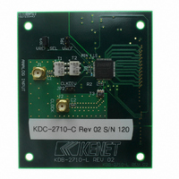
Manufacturer Part Number
KDC2710CEVAL
Description
DAUGHTER CARD FOR KAD2710
Manufacturer
Intersil
Series
FemtoCharge™r
Datasheets
1.KAD2710C-10Q68.pdf
(16 pages)
2.KMB-001LEVALZ.pdf
(7 pages)
3.KDC5514EVALZ.pdf
(9 pages)
Specifications of KDC2710CEVAL
Number Of Adc's
1
Number Of Bits
10
Sampling Rate (per Second)
275M
Data Interface
Parallel
Inputs Per Adc
1 Differential
Input Range
1.5 Vpp
Power (typ) @ Conditions
261mW @ 275MSPS
Voltage Supply Source
Single Supply
Operating Temperature
-40°C ~ 85°C
Utilized Ic / Part
KAD2710C-27, KMB001 Motherboard
For Use With
KMB001LEVAL - MOTHERBOARD FOR LVDS ADC CARD
Lead Free Status / RoHS Status
Lead free / RoHS Compliant


INP
INN
This relationship shows the SNR that would be achieved if
clock jitter were the only non-ideal factor. In reality,
achievable SNR is limited by internal factors such as
linearity, aperture jitter and thermal noise. Internal aperture
jitter is the uncertainty in the sampling instant shown in
Figure 1. The internal aperture jitter combines with the input
clock jitter in a root-sum-square fashion, since they are not
statistically correlated, and this determines the total jitter in
the system. The total jitter, combined with other noise
sources, then determines the achievable SNR.
Equivalent Circuits
Intersil products are sold by description only. Intersil Corporation reserves the right to make changes in circuit design, software and/or specifications at any time without
notice. Accordingly, the reader is cautioned to verify that data sheets are current before placing orders. Information furnished by Intersil is believed to be accurate and
reliable. However, no responsibility is assumed by Intersil or its subsidiaries for its use; nor for any infringements of patents or other rights of third parties which may result
from its use. No license is granted by implication or otherwise under any patent or patent rights of Intersil or its subsidiaries.
AVDD3
AVDD3
All Intersil U.S. products are manufactured, assembled and tested utilizing ISO9000 quality systems.
FIGURE 28. ANALOG INPUTS
2pF
2pF
Intersil Corporation’s quality certifications can be viewed at www.intersil.com/design/quality
For information regarding Intersil Corporation and its products, see www.intersil.com
Φ
F 1
Φ
F 1
14
Φ
F 2
Φ
F 2
DATA
Csamp
Csamp
0.3pF
0.3pF
FIGURE 30. LVCMOS OUTPUTS
Pipeline
Pipeline
Charge
Charge
OVDD
To
To
KAD2710C
OVDD
Digital Outputs
Data is output on a parallel bus with LVCMOS drivers.
The output format (Binary or Two’s Complement) is selected
via the 2SC pin as shown in Table 3.
CLKN
CLKP
AVDD (or unconnected)
AVDD2
AVDD2
2SC PIN
D[9:0]
AVSS
TABLE 3. 2SC PIN SETTINGS
FIGURE 29. CLOCK INPUTS
Two’s Complement
AVDD2
MODE
Binary
December 5, 2008
Generation
To Clock
FN6814.0
Related parts for KDC2710CEVAL
Image
Part Number
Description
Manufacturer
Datasheet
Request
R

Part Number:
Description:
Intersil Corporation [CMOS Serial Controller Interface]
Manufacturer:
Intersil Corporation
Datasheet:
Part Number:
Description:
Manufacturer:
Intersil Corporation
Datasheet:
Part Number:
Description:
357-036-542-201 CARDEDGE 36POS DL .156 BLK LOPRO
Manufacturer:
Intersil Corporation
Datasheet:
Part Number:
Description:
1024-Word x 4-Bit LSI Static RAM
Manufacturer:
Intersil Corporation
Datasheet:
Part Number:
Description:
General Purpose NPN Transistor Arrays FN341.4
Manufacturer:
Intersil Corporation
Datasheet:
Part Number:
Description:
CMOS 16-Bit Microprocessor
Manufacturer:
Intersil Corporation
Datasheet:
Part Number:
Description:
Manufacturer:
Intersil Corporation
Datasheet:
Part Number:
Description:
Manufacturer:
Intersil Corporation
Datasheet:
Part Number:
Description:
Manufacturer:
Intersil Corporation
Datasheet:
Part Number:
Description:
Manufacturer:
Intersil Corporation
Datasheet:
Part Number:
Description:
CMOS 6-Bit Latch and Decoder Memory Interfaces
Manufacturer:
Intersil Corporation
Datasheet:
Part Number:
Description:
CA3046General Purpose NPN Transistor Arrays
Manufacturer:
Intersil Corporation
Datasheet:
Part Number:
Description:
Manufacturer:
Intersil Corporation
Datasheet:
Part Number:
Description:
TR909 DLC/FLC SLIC with Low Power Standby
Manufacturer:
Intersil Corporation
Datasheet:
Part Number:
Description:
Manufacturer:
Intersil Corporation
Datasheet: