KDC5512-Q48EVAL Intersil, KDC5512-Q48EVAL Datasheet - Page 8
KDC5512-Q48EVAL
Manufacturer Part Number
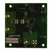
KDC5512-Q48EVAL
Description
DAUGHTER CARD FOR KAD5512
Manufacturer
Intersil
Series
FemtoCharge™r
Datasheets
1.KAD5512P-25Q72.pdf
(36 pages)
2.KMB-001LEVALZ.pdf
(7 pages)
3.KDC5514EVALZ.pdf
(9 pages)
Specifications of KDC5512-Q48EVAL
Number Of Adc's
1
Number Of Bits
12
Sampling Rate (per Second)
250M
Data Interface
Parallel
Inputs Per Adc
1 Differential
Input Range
1.5 Vpp
Voltage Supply Source
Single Supply
Operating Temperature
-40°C ~ 85°C
Utilized Ic / Part
KAD5512P-25, KMB001 Motherboard
For Use With
KMB001LEVAL - MOTHERBOARD FOR LVDS ADC CARD
Lead Free Status / RoHS Status
Lead free / RoHS Compliant


Table of Contents
Absolute Maximum Ratings .............................. 9
Thermal Information ........................................ 9
Recommended Operating Conditions ................ 9
Electrical Specifications. ................................... 9
Digital Specifications ...................................... 12
Timing Diagrams ............................................. 13
Switching Specifications .................................. 14
Typical Performance Curves ............................ 15
Theory of Operation......................................... 18
Functional Description..................................... 18
Power-On Calibration ...................................... 18
User-Initiated Reset ....................................... 19
Analog Input ................................................. 19
VCM Output................................................... 20
Clock Input ................................................... 20
Jitter ............................................................ 20
Voltage Reference .......................................... 21
Digital Outputs .............................................. 21
Over Range Indicator...................................... 21
Power Dissipation........................................... 21
Nap/Sleep ..................................................... 21
Data Format .................................................. 22
8
KAD5512P
Serial Peripheral Interface .............................. 24
Equivalent Circuits .......................................... 30
ADC Evaluation Platform ................................. 31
Layout Considerations..................................... 31
General PowerPAD Design Considerations ...... 31
Definitions....................................................... 32
Revision History .............................................. 33
Products.......................................................... 34
Package Outline Drawing ............................... 35
Package Outline Drawing ............................... 36
SPI Physical Interface .................................... 24
SPI Configuration .......................................... 24
Device Information ........................................ 25
Indexed Device Configuration/Control .............. 25
Global Device Configuration/Control ................. 26
Device Test................................................... 27
72 Pin/48 Pin Package Options ........................ 27
SPI Memory Map ........................................... 28
PCB Layout Example ...................................... 31
Split Ground and Power Planes ........................ 31
Clock Input Considerations ............................. 31
Exposed Paddle ............................................. 31
Bypass and Filtering....................................... 31
LVDS Outputs ............................................... 31
LVCMOS Outputs ........................................... 31
Unused Inputs .............................................. 31
October 1, 2010
FN6807.4
Related parts for KDC5512-Q48EVAL
Image
Part Number
Description
Manufacturer
Datasheet
Request
R

Part Number:
Description:
DAUGHTER CARD FOR KDC5512
Manufacturer:
Intersil
Datasheet:

Part Number:
Description:
DAUGHTER CARD FOR KAD5512
Manufacturer:
Intersil
Datasheet:

Part Number:
Description:
Intersil Corporation [CMOS Serial Controller Interface]
Manufacturer:
Intersil Corporation
Datasheet:
Part Number:
Description:
Manufacturer:
Intersil Corporation
Datasheet:
Part Number:
Description:
357-036-542-201 CARDEDGE 36POS DL .156 BLK LOPRO
Manufacturer:
Intersil Corporation
Datasheet:
Part Number:
Description:
1024-Word x 4-Bit LSI Static RAM
Manufacturer:
Intersil Corporation
Datasheet:
Part Number:
Description:
General Purpose NPN Transistor Arrays FN341.4
Manufacturer:
Intersil Corporation
Datasheet:
Part Number:
Description:
CMOS 16-Bit Microprocessor
Manufacturer:
Intersil Corporation
Datasheet:
Part Number:
Description:
Manufacturer:
Intersil Corporation
Datasheet:
Part Number:
Description:
Manufacturer:
Intersil Corporation
Datasheet:
Part Number:
Description:
Manufacturer:
Intersil Corporation
Datasheet:
Part Number:
Description:
Manufacturer:
Intersil Corporation
Datasheet:
Part Number:
Description:
CMOS 6-Bit Latch and Decoder Memory Interfaces
Manufacturer:
Intersil Corporation
Datasheet:
Part Number:
Description:
CA3046General Purpose NPN Transistor Arrays
Manufacturer:
Intersil Corporation
Datasheet:
Part Number:
Description:
Manufacturer:
Intersil Corporation
Datasheet: