CDB5581 Cirrus Logic Inc, CDB5581 Datasheet - Page 5
CDB5581
Manufacturer Part Number
CDB5581
Description
BOARD EVAL FOR CS5581 ADC
Manufacturer
Cirrus Logic Inc
Type
A/Dr
Datasheet
1.CDB5581.pdf
(26 pages)
Specifications of CDB5581
Number Of Adc's
1
Number Of Bits
16
Sampling Rate (per Second)
200k
Data Interface
Serial
Inputs Per Adc
2 Single
Input Range
±2.048 V
Power (typ) @ Conditions
85mW @ 200kSPS
Voltage Supply Source
Dual ±
Operating Temperature
-40°C ~ 85°C
Utilized Ic / Part
CS5581
Product
Data Conversion Development Tools
Conversion Rate
200 KSPS
Resolution
16 bit
Maximum Clock Frequency
16 MHz
Interface Type
SPI
Supply Voltage (max)
3.3 V
Supply Voltage (min)
- 2.5 V
For Use With/related Products
CS5581
Lead Free Status / RoHS Status
Contains lead / RoHS non-compliant
Lead Free Status / RoHS Status
Lead free / RoHS Compliant, Contains lead / RoHS non-compliant
Other names
598-1559


2. QUICK START
The
configure the
DS796DB3
1. Verify that the power supplies are off.
2. Connect the power supplies to the CDB5581 as shown in Table 1 on page 6.
3. Verify that the power is off to the analog input signal & control signal sources.
4. Connect the analog input signal source to the evaluation board per Table 2 on page 6. Verify from Table 4
5. Configure the CDB5581 by connecting the control signal sources to the evaluation board as shown in
6. Make connections to the SPI™ serial port connector as shown in Table 5 on page 8. The CS5581 ADC
7. Turn on the power supplies to the evaluation board.
8. Apply power to the signal source.
9. Press the Reset switch on the evaluation board.
10. The CS5581 ADC's SPI™ serial port should now be communicating data.
CDB5581
on page 8 that the analog input channel selected is IN_A.
Table 3 on page 7. Apply logic-level inputs as required to override the resistor pull-ups/pull-downs.
serial port is configured by default to operate in the SSC (Synchronous Self Clocking) mode. Refer to the
CS5581 data sheet for more information on serial communication modes and signal timing.
NOTES:
1. Shaded boxes marked with "OPT. CONFIG." are not necessary for operation in an end user product.
2. Calibration function has been removed from the device but still appears on the PCB. J2 must be shorted (grounded)
for proper operation. See Appendix E for details.
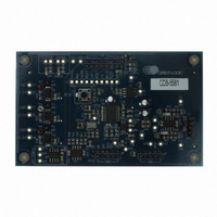
CDB5581
evaluation board is designed to interface with a data acquisition system. To connect and
DC Supply
Buffer Enable
perform the following initialization procedure:
ADC Reset
Calibrate
Figure 2. CDB5581 Board Layout
2
Master/Slave SPI
Signals to ADC & Mux
ADC MCLK Out
4.096 V Reference
Analog Inputs
CDB5581
5
Related parts for CDB5581
Image
Part Number
Description
Manufacturer
Datasheet
Request
R

Part Number:
Description:
Development Kit
Manufacturer:
Cirrus Logic Inc
Datasheet:
Part Number:
Description:
Development Kit
Manufacturer:
Cirrus Logic Inc
Datasheet:


Part Number:
Description:
High-efficiency PFC + Fluorescent Lamp Driver Reference Design
Manufacturer:
Cirrus Logic Inc
Datasheet:
Part Number:
Description:
Development Kit
Manufacturer:
Cirrus Logic Inc
Datasheet:
Part Number:
Description:
Development Kit
Manufacturer:
Cirrus Logic Inc
Datasheet:

Part Number:
Description:
Development Kit
Manufacturer:
Cirrus Logic Inc
Datasheet:
Part Number:
Description:
Development Kit
Manufacturer:
Cirrus Logic Inc
Datasheet:
Part Number:
Description:
Development Kit
Manufacturer:
Cirrus Logic Inc
Datasheet:
Part Number:
Description:
Development Kit
Manufacturer:
Cirrus Logic Inc
Datasheet:

Part Number:
Description:
EVALUATION BOARD FOR CS8427
Manufacturer:
Cirrus Logic Inc
Datasheet:

Part Number:
Description:
BOARD EVAL FOR CS8416 RCVR
Manufacturer:
Cirrus Logic Inc
Datasheet:

Part Number:
Description:
EVALUATION BOARD FOR CS8420
Manufacturer:
Cirrus Logic Inc
Datasheet:

Part Number:
Description:
KIT DEVELOPMENT EP9315 ARM9
Manufacturer:
Cirrus Logic Inc
Datasheet:

Part Number:
Description:
KIT DEVELOPMENT EP9302 ARM9
Manufacturer:
Cirrus Logic Inc
Datasheet: