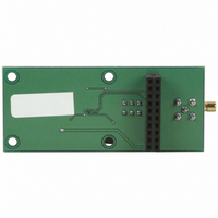
AD7940-DBRD Analog Devices Inc, AD7940-DBRD Datasheet - Page 19

AD7940-DBRD
Manufacturer Part Number
AD7940-DBRD
Description
BOARD EVAL FOR AD7940 STAMP SPI
Manufacturer
Analog Devices Inc
Datasheet
1.AD7940BRJZ-REEL7.pdf
(20 pages)
Specifications of AD7940-DBRD
Number Of Adc's
1
Number Of Bits
14
Sampling Rate (per Second)
100k
Data Interface
Serial
Inputs Per Adc
1 Single Ended
Input Range
0 ~ Vdd
Power (typ) @ Conditions
17mW @ 100kSPS & 5 V
Voltage Supply Source
Single Supply
Operating Temperature
-40°C ~ 85°C
Utilized Ic / Part
AD7940
Lead Free Status / RoHS Status
Lead free / RoHS non-compliant
APPLICATION HINTS
GROUNDING AND LAYOUT
The printed circuit board that houses the AD7940 should be
designed such that the analog and digital sections are separated
and confined to certain areas of the board. This facilitates the
use of ground planes that can be separated easily. A minimum
etch technique is generally best for ground planes, since it gives
the best shielding. Digital and analog ground planes should be
joined at only one place. If the AD7940 is in a system where
multiple devices require an AGND to DGND connection, the
connection should still be made at one point only, a star ground
point that should be established as close as possible to the AD7940.
Avoid running digital lines under the device since these will
couple noise onto the die. The analog ground plane should be
allowed to run under the AD7940 to avoid noise coupling. The
power supply lines to the AD7940 should use as large a trace as
possible to provide low impedance paths and reduce the effects
of glitches on the power supply line. Fast switching signals, such
as clocks, should be shielded with digital ground to avoid radi-
ating noise to other sections of the board, and clock signals
should never be run near the analog inputs. Avoid crossover of
digital and analog signals. Traces on opposite sides of the board
should run at right angles to each other, which will reduce the
effects of feedthrough through the board. A microstrip tech-
nique is by far the best but is not always possible with a double-
sided board. In this technique, the component side of the board
is dedicated to ground planes while the signals are placed on the
solder side.
Rev. 0 | Page 19 of 20
Good decoupling is also very important. All analog supplies
should be decoupled with 10 µF tantalum in parallel with 0.1 µF
capacitors to AGND, as discussed in the Typical Connection
Diagram section. To achieve the best performance from these
decoupling components, the user should attempt to keep the
distance between the decoupling capacitors and the V
GND pins to a minimum, with short track lengths connecting
the respective pins.
EVALUATING THE AD7940 PERFORMANCE
The recommended layout for the AD7940 is outlined in the
evaluation board for the AD7940. The evaluation board package
includes a fully assembled and tested evaluation board, docu-
mentation, and software for controlling the board from the PC
via the evaluation board controller. The evaluation board con-
troller can be used in conjunction with the AD7940 evaluation
board, as well as many other Analog Devices evaluation boards
ending in the CB designator, to demonstrate/evaluate the ac and
dc performance of the AD7940.
The software allows the user to perform ac (fast Fourier trans-
form) and dc (histogram of codes) tests on the AD7940. The
software and documentation are on a CD shipped with the
evaluation board.
AD7940
DD
and


