NCP348GEVB ON Semiconductor, NCP348GEVB Datasheet - Page 3
NCP348GEVB
Manufacturer Part Number
NCP348GEVB
Description
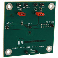
EVAL BOARD FOR NCP348G
Manufacturer
ON Semiconductor
Specifications of NCP348GEVB
Design Resources
NCP348G EVB BOM NCP348GEVB Gerber Files NCP348G EVB Schematic
Main Purpose
Overvoltage Protection
Embedded
No
Utilized Ic / Part
NCP348
Primary Attributes
Overvoltage Protection up to 28V
Secondary Attributes
Overvoltage Lockout (OVLO), Undervoltage Lockout (UVLO)
Silicon Manufacturer
On Semiconductor
Silicon Core Number
NCP348
Kit Application Type
Power Management
Application Sub Type
Overvoltage Protection
Rohs Compliant
No
Lead Free Status / RoHS Status
Lead free / RoHS Compliant
For Use With/related Products
NCP348G
Other names
NCP348GEVBOS


Stresses exceeding Maximum Ratings may damage the device. Maximum Ratings are stress ratings only. Functional operation above the
Recommended Operating Conditions is not implied. Extended exposure to stresses above the Recommended Operating Conditions may affect
device reliability.
1. The R
2. Human Body Model, 100 pF discharged through a 1.5 kW resistor following specification JESD22/A114.
3. Machine Model, 200 pF discharged through all pins following specification JESD22/A115.
PIN FUNCTION DESCRIPTION
MAXIMUM RATINGS
Pin No.
PAD1
PAD2
Minimum Voltage (IN to GND)
Minimum Voltage (All others to GND)
Maximum Voltage (IN to GND)
Maximum Voltage (All others to GND)
Maximum Current (UVLO<V
Thermal Resistance, Junction−to−Air (Note 1)
Operating Ambient Temperature Range
Storage Temperature Range
Junction Operating Temperature
ESD Withstand Voltage (IEC 61000−4−2) (input only) when bypassed with 1.0 mF capacitor
Moisture Sensitivity
189 °C/W with 400 mm
10
Human Body Model (HBM), Model = 2 (Note 2)
Machine Model (MM) Model = B (Note 3)
1
4
5
2
3
6
7
8
9
qJA
Symbol
is highly dependent on the PCB heat sink area (connected to pad 2). As example R
FLAG
GND
OUT
NC
NC
EN
IN
Function
OUTPUT
OUTPUT
2
POWER
POWER
INPUT
.
OPEN
OPEN
IN
<OVLO)
Fault Indication Pin.
This pin allows an external system to detect a fault on IN pin.
The FLAG pin goes low when input voltage exceeds OVLO threshold or drop below UVLO threshold.
Since the FLAG pin is open drain functionality, an external pull up resistor to V
Enable Pin.
The device enters in shutdown mode when this pin is tied to a high level. In this case the output is
disconnected from the input.
To allow normal functionality, the EN pin shall be connected to GND to a pull down or to a I/O pin.
This pin does not have an impact on the fault detection.
Input Voltage Pin.
This pin is connected to the power supply.
The device system core is supplied by this input.
A 1 mF low ESR ceramic capacitor, or larger, must be connected between this pin and GND.
The three IN pins must be hardwired to common supply.
Ground
Output Voltage Pin.
This pin follows IN pin when “no fault” is detected.
The output is disconnected from the V
threshold or above OVLO threshold.
The two OUT pins must be hardwired to common supply.
No Connect
No Connect
PAD1, under the device. See PCB recommendations page 10.
Can be shorted to GND.
The PAD2 is electrically connected to the internal NMOS drain and connected to Pins 4 and 5.
See PCB recommendations page 10.
Rating
http://onsemi.com
3
in
power supply when the input voltage is under the UVLO
Description
qJA
is 268 °C/W with 30 mm
Symbol
Vmax
Vmin
Vmax
Vmin
Imax
Vesd
R
MSL
T
T
T
qJA
stg
A
J
in
in
15 Air, 8.0 Contact
−65 to +150
−40 to +85
Level 1
Value
CC
2000
−0.3
−0.3
280
150
200
7.0
2.0
30
must be added.
2
(copper 35 mm) and
°C/W
Unit
°C
°C
°C
kV
V
V
V
V
A
V
V
−
Related parts for NCP348GEVB
Image
Part Number
Description
Manufacturer
Datasheet
Request
R

Part Number:
Description:
Positive Overvoltage Protection Controller with Internal Low R_ON NMOS FET and Status FLAG
Manufacturer:
ONSEMI [ON Semiconductor]
Datasheet:

Part Number:
Description:
ON Semiconductor [VOLTAGE REGULATOR]
Manufacturer:
ON Semiconductor
Datasheet:
Part Number:
Description:
357-036-542-201 CARDEDGE 36POS DL .156 BLK LOPRO
Manufacturer:
ON Semiconductor
Datasheet:
Part Number:
Description:
357-036-542-201 CARDEDGE 36POS DL .156 BLK LOPRO
Manufacturer:
ON Semiconductor
Datasheet:
Part Number:
Description:
357-036-542-201 CARDEDGE 36POS DL .156 BLK LOPRO
Manufacturer:
ON Semiconductor
Datasheet:
Part Number:
Description:
357-036-542-201 CARDEDGE 36POS DL .156 BLK LOPRO
Manufacturer:
ON Semiconductor
Datasheet:
Part Number:
Description:
357-036-542-201 CARDEDGE 36POS DL .156 BLK LOPRO
Manufacturer:
ON Semiconductor
Datasheet:
Part Number:
Description:
357-036-542-201 CARDEDGE 36POS DL .156 BLK LOPRO
Manufacturer:
ON Semiconductor
Datasheet:
Part Number:
Description:
357-036-542-201 CARDEDGE 36POS DL .156 BLK LOPRO
Manufacturer:
ON Semiconductor
Datasheet:
Part Number:
Description:
357-036-542-201 CARDEDGE 36POS DL .156 BLK LOPRO
Manufacturer:
ON Semiconductor
Datasheet:
Part Number:
Description:
357-036-542-201 CARDEDGE 36POS DL .156 BLK LOPRO
Manufacturer:
ON Semiconductor
Datasheet:
Part Number:
Description:
357-036-542-201 CARDEDGE 36POS DL .156 BLK LOPRO
Manufacturer:
ON Semiconductor
Datasheet:
Part Number:
Description:
Manufacturer:
ON Semiconductor
Datasheet:
Part Number:
Description:
Manufacturer:
ON Semiconductor
Datasheet: