M3A-0033 Renesas Electronics America, M3A-0033 Datasheet
M3A-0033
Specifications of M3A-0033


Related parts for M3A-0033


M3A-0033 Summary of contents
Page 1
M66291GP Evaluation Board ...
Page 2
Renesas Technology Corporation puts the maximum effort into making semiconductor products better and more reliable, but there is always the possibility that trouble may occur with them. Trouble with semiconductors may lead to personal injury, fire or property damage. Remember ...
Page 3
... Quitting FlashStart ..................................................................................................................... 12 5.5 Uninstalling KD308 ....................................................................................................................13 5.6 Uninstalling KNC308WA ...........................................................................................................13 5.7 Uninstalling FlashStart .............................................................................................................13 5.8 Referencing Electronic Manuals.............................................................................................13 Chapter 6. Modification of the Setting of the M3A-0033...............................................14 6.1 Changing Power Supply Setting .............................................................................................14 6.2 Setting DMA Transfer Using *DREQ.......................................................................................14 6.3 Jumper Setting for Enabling UART0 (CN6) Communication ............................................15 Contents ...
Page 4
... Chapter 7. Modification of the Monitor Program ..........................................................16 7.1 Setting for Modification.............................................................................................................16 7.2 How to Modify the Monitor Program .......................................................................................16 Chapter8. M3A-0033 Specification ................................................................................18 8.1 Block Diagram .............................................................................................................................18 8.2 M16C/80 Part ................................................................................................................................19 8.3 Monitor Program Specification And Memory Map Every M16C/80 CPU Mode................19 8.4 KD308 Communication Specification ....................................................................................20 8.5 Expansion Bus Interface ...........................................................................................................21 8 ...
Page 5
... Chapter 1. Outline M3A-0033 is a development board for evaluating Renesas original USB ASSP M66291GP, and combinating M3A-0033 mounted Renesas original 16bits microcomputer M16C/80 and M3A-0032 (enclosure), the chip can be evaluated easily. Moreover, since the debugging monitor is built in the microcomputer, an expensive debugger is not needed ...
Page 6
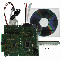
... M66291GP evaluation board (M3A-0033) 7. M66291GP utility board (M3A-0032) 8. Power supply cable 9. power supply (No package) Regulated DC 10. Host PC (No package) 11. USB cable (No package) In addition, user application board is connectable with M3A-0033. 3.2 System Configuration Figure Host-PC USB cable M3A-0032 M66291GP M3A-0033 PC for development ...
Page 7
... M66291GP Evaluation Board 3.3 Top View Top view of M3A-0033 is shown in Fig. 3-2, and explanation of main units is shown in Table 3-1. (Power supply plug) JP6 JP5 JP18 JP12 JP3 JP4 CN8, CN9 (Connectors for M3A-003) : This part is not mounted. Please locate as necessary. Table. 3-1 M3A-0033 Main Units ...
Page 8
... M66291GP Evaluation Board 3.4 Jumper Switch Setup (JPx) Jumper switches setup of M3A-0033 are shown in Table 3-2. Table 3-2 Jumper switch setup of M3A-0033 JP Name Contents JP1 Flash memory Short: Programming to internal flash memory of M16C/80 by FlashStart. (Note1) programming Open: Debugging by KD308 or running user programmed by FlashStart(Default) ...
Page 9
... M66291GP Evaluation Board 3.5 Slide Switch (SW1, SW2) Setup of slide switches are shown in Table 3-3. Table 3-3 M3A-0033 Slide Switch SW Name Setting SW1 MAX3241E Set power supply to MAX3241E (U5) to ON/OFF. Power supply Usually, please set to “ON” side. “ON” “OFF” ...
Page 10
... M3A-0033 Setup Please set jumpers as shown in Figure. 4-1. Jumpers are already set at the time of product shipment. 4.2 M3A-0032 Setup Please set jumpes as shown in Figure. 4-2. Jumpers are already set at the time of product shipment. Figure. 4-1 M3A-0033 Jumper Setup JP2 JP3 JP1 Figure ...
Page 11
... Note: Make sure CN2 is connected to CN8 and CN3 is connected to CN9. 2. External power supply Connect a 5.0V external regulated power supply to plug (CN1) of M3A-0033. Note: Be sure to observe the correct polarity and voltage. The M3A-0033 board has no reverse polarity protection. 3. Code development PC Connect the PC to CN3 of M3A-0033 using the serial cable provided. ...
Page 12
... The Init dialog box is detailed in KD308's manual. Here, set the following item to ensure that KD308 starts up normally. When you have finished setting the above, click on the <OK> button in the Init dialog box. If communication is performed normally, KD308 starts up automatically and a window like the one shown in Figure 5-2 appears. Figure 5-1 Init Window - 8 - M3A-0033 ...
Page 13
... M66291GP Evaluation Board If M3A-0033 fails to communicate with the personal computer, an error dialog box like the one shown in Figure 5-3 appears. Figure 5-3 Example of Error Dialog Box at Start-up When you click on the <OK> button in this error dialog box, the Init dialog box pops up again. If this error dialog box is displayed, refer to Section 9 ...
Page 14
... Prevent MS-DOS -based programs from detecting Windows. 4)Close the DOS window, then execute the command again. <If version numbers are not displayed...> Check to see if each command (listed in Section 5.3.1) is expanded correctly in the directory you have specified for BIN308 M3A-0033 ...
Page 15
... It clicks on"Flashsta.exe" in the copied file double for the start. When FlashStart starts, the window of the figure 5-5 opens. "Select Program" choose "Internal flash memory". Setup RS232C to use more than Pull Down List. When click <OK> button, a windows appears.(Figure 5-6) Figure 5-5 Set Baudrate Window Figure 5-6 ID Check Window - 11 - M3A-0033 ...
Page 16
... M66291GP Evaluation Board Detail operation of ID check Window and FlashStart check Flash Start's manual. When Figure 5-7 appears , please check to connection between Serial interface cable and M3A-0033. Figure 5-7 Connection Error Window 5.4.3. Quitting FlashStart When Flash Start quit. click <Exit> on Figure 5-8. ...
Page 17
... Start up the installer on the CD-ROM holding the product. (2) Install Adobe Acrobat Reader according to what are contained in the Readme file. The user can download Adobe Acrobat Reader from the home page of Adobe Systems Incorporated. For latest information as to Adobe Acrobat Reader the following URLs. http://www.adobe.com - 13 - M3A-0033 ...
Page 18
... Chapter 6. Modification of the Setting of the M3A-0033 6.1 Changing Power Supply Setting The power supply to M3A-0033 and M3A-0032, “External power supply (CN1)” or “ Vbus power supply on USB line” are selectable. Please set up the jumper as Table 6-1. Table 6-1 Jumper Setting for Supplying Origin of External Power Supply ...
Page 19
... RTS pin of CN6 is connected to P80 pin of M16C/80 (via MAX3241E) (Note) JP21 Short-circuit CTS pin of CN6 is connected to CTS0 pin of M16C/80 (via MAX3241E) Note: Software control is required for RTS handshake. Explanation TxD pin of CN6 is connected to TXD0 pin of M16C(via MAX3241E) RxD pin of CN6 is connected to RXD0 pin of M16C (via MAX3241E M3A-0033 ...
Page 20
... M66291GP Evaluation Board Chapter 7. Modification of the Monitor Program 7.1 Setting for Modification When changing the oscillator of M3A-0033 into 20MHz necessary to change the monitor program of internal flash memory of M16C/80. The change method of monitor program is shown below. (1) Change and create monitor program. Please refer section “7.2” about change method. In addition, the execution file (20MHz correspondence version monitor program) is prepared in \ENGLISH\PROGRAM\MONITOR\MOT (20MHz) folder attached CD-ROM, please use it ...
Page 21
... MOV.B #00000010B, MCD; divide-by-2 mode 141; MOV.B #00000011B, MCD; divide-by-3 mode 142 MOV.B #00000100B, MCD; divide-by-4 mode 143; MOV.B #00000110B, MCD; divide-by-6 mode Please set the division mode as Table 7-4. When 20MHz Divide-by-4 Please set the division mode as Table 7- M3A-0033 ...
Page 22
... M66291GP Evaluation Board Chapter8. M3A-0033 Specification 8.1 Block Diagram The block diagram of M3A-0033 is shown in Figure 8-1. U6 not mounted 5.0V Reg1 Reg2 (3.3V) (3.3V 5.0V External JP5 Power supply JP7 short-circuit Vbus M3A-0032 EXIOVcc or EX_Vcc M3A-0029B RST TC1 JP14 JP15 Dreq1 6629x ...
Page 23
... Used when debugger communication Single step Used when step execution of user program Address-match Used when software break execution (2) Interface with User Program Controlling the stack information executed by REIT command, it starts user program from monitor program. SP-4 SP-3 SP-2 SP-1 PC(L) PC(M) FLG(L) FLG(H) PC( M3A-0033 ...
Page 24
... M66291GP Evaluation Board (3) Memory Map In M3A-0033, M16C/80 can operate in the mode 1 of memory expansion mode. The bus width is 16 bits (separate bus). The memory map is shown below. 000000H SFR area 000400H Internal RAM area Internal reserved area 008000H *CS1 (2M bytes) 200000H ...
Page 25
... HOLD, HLDA, BCLK, ALE)............5 -UART1 ( ......................................................................... -General-purpose ports ( -P9 , P10 -P10 ............................................................ -Reset signal (*RESET) ..................................................................1 -External interrupt request signal (*INT0 to *INT2)....................3 -Vcc*2/GND*2/AVCC/AVSS/Vref ...............................................7 ............................................................................................................ The numbers of expansion connector pins are 96 pins. The assignment of expansion connector pins is shown in Table 8- M3A-0033 ...
Page 26
... A6 14C 61 A9 15C 58 A12 16C 55 A15 17C 52 A18 18C 48 *CS1 19C 46 *WRL 20C 43 P53/BLCK 21C 40 P56 22C 37 P61 23C 34 P64 24C 31 P67/TXD1 25C 28 P72 26C 25 P75 27C 22 P80 28C 19 *INT1 29C 12 *RESET 30C 7 P90 31C 4 P93 32C - (GND M3A-0033 ...
Page 27
... M66290AGP Pin NO Pin name Pin NO - (GND) 40 D15/A0 (JP3=D15) 39 D14/P6 38 D13/P5 37 D12/P4 34 D11/P3 33 D10/P2 32 D9/P1 31 D8/P0 - (GND (GND) - (GND) - (NC) - (NC) 41 *HWR/ (JP2=16bit) *BYTE 5 VBUS - (EXIOVCC) - (EXIOVCC M3A-0033 Pin name - (GND) 40 D15 39 D14 38 D13 37 D12 34 D11 33 D10 (GND (GND) - (GND) - (NC) - (NC) - (NC) - (NC) - (NC) - (NC) ...
Page 28
... (GND) - (EX_VCC) - (EX_VCC) - (NC) 40 D15/A0 (JP3 *TC1 11 *INT1/SOF 8 *Dack1 9 *Dreq1 - 24 - M3A-0033 Pin name 44 *WR - (GND) 43 *RD - (GND) 45 *CS 8/46 *TRST /*RST 47 *Dreq 48 *Dack 42 *INT - (GND) - (GND (GND) - (VCC) - (VCC) (NC) (NC) (NC) (NC) (NC) (NC) ...
Page 29
... Write to the D flag is ignored (Always D flag flag is 1). Do not clear a flag in user program. Do not make changes. Do not change bits and 6. Do not write any data to this register. Do not read this register. Do not modify this register M3A-0033 Change in user program Changeable Changeable Changeable Changeable Changeable ...
Page 30
... Restrictions on Stop Mode or Wait Mode The monitor program cannot be run in STOP modes and WAIT modes. Can't be changed STOP modes or WAIT modes in user program. Specification for Monitor program Use inhibited (Note1) Use inhibited (Note1) Use inhibited Use inhibited Use inhibited Use inhibited FFFFFCH -FFFFFFH - 26 - M3A-0033 ...
Page 31
... From the INT instruction, you cannot successively step through the internal processing of the INT instruction. <Example> NOP NOP INT #3 STEP NOP JMP MAIN INT_3: NOP Address at which program execution ought to stop NOP REIT Interruption NOP NOP REIT Here execute STEP. Skipped over when STEP is executed M3A-0033 ...
Page 32
... M3A-0033 hardware is correctly set up (2) Whether cable is firmly connected and whether the power is turned on. (3) Whether the serial port set in the Init dialog box matches the actual serial port where the M3A-0033 is connected. 9.9 Corrective Action when Communication Error Occurs During Debug If a communication error occurs during debug, one probable cause is that the monitor program is made to go wild by the user program (ex, user programs runaway or access to monitor area) ...
Page 33
... In the case of connecting M3A-0029B, please set JP6 of M3A-0033 to "3.3V" side. Note: If the above-mentioned jumper setup is not done when using M3A-0032 and M3A-0029B, M3A-0033 and M3A-0032 and M3A-0029B may become impossible to use, please be careful of use. 9.13 Reset Signal When JP11 is short-circuited, you can program the hardware-reset of the M66291 low pulsing P7 Please refer the M66291 data sheet for the timing. Note: When you program doesn’ ...
Page 34
... Monitor program (16K) Vector area( fixed) Figure 9-1 Memory Map 2 Explanation *DACK0 pin of M66291GP is assigned to *CS2 pin of M 16C/80. *DACK1 pin of M66291GP is assigned to *CS3 pin of M 16C/80 M3A-0033 USB enable register FFBE00H Unusable area FFC000H Monitor program FFFE00H Special page Vector table ...
Page 35
... M66291GP Evaluation Board M3A-0033 Instruction Manual © 2002(2003) RENESAS TECHNOLOGY CORPORATION AND RENESAS SOLUTIONS CORPORATION No reproduction without permission. Reproduction or publication of part of or entire content of this document in any form, without express permission by the publisher, is strictly prohibited. 2003-07-01 ...
Page 36
... Renesas NEC MAXIM Murata 10MHz ALPS JST OKI OMRON Note-1 HIROSE Honda Rohm MAC8 Note-1 MAC8 Note-1 COPAL COPAL Rohm 100Kohm Rohm 15Kohm Rohm 22Kohm Rohm 10Kohm Rohm 68ohm Rohm 220ohm Rohm 0ohm TYTLE M66291GP(USB ASSP)Evaluation Board DRAWING PPL –M3A-0033A NO. (1/2) ...
Page 37
... GRM40CH471J50V LC-2-G(Red) LC-2-G(Yellow) LC-2-G(White) LC-2-G(Black) SML-210MT SML-210DT 61AAA0091A 9AA9A0187A GRM40F334Z50V Notes Manufacture Rohm 100ohm MEC Nichicon Nichicon MEC MEC Murata 0 Murata 30pF/50V Murata 470pF/50V MAC8 MAC8 MAC8 MAC8 Rohm Rohm ALPS ALPS Murata 0. M66291GP(USB ASSP)Evaluation Board TYTLE PPL –M3A-0033A DRAWING NO. (2/2) ...
Page 38
Following devices are not mounted. U6, C2, R24, R25, R26 U1 16Pin U1 62Pin Note: 1) The pins of JP7 are shorted. Please cut the shorted pattern, when you mount JP7. U1 14Pin U1 64Pin 2) The pins of JP8 ...
Page 39
SHORTED BY PATTERN ORANGE LED SHORTED BY PATTERN FEB GREEN LED VOLTAGE SUPPLY SELECT CIRCUIT CN5 U1 4PIN U1 3PIN U1 7PIN U1 6PIN U1 12PIN U1 11PIN U1 19PIN U1 18PIN U1 22PIN U1 21PIN U1 25PIN U1 24PIN ...