SD384EVK National Semiconductor, SD384EVK Datasheet - Page 2
SD384EVK
Manufacturer Part Number
SD384EVK
Description
BOARD EVAL CABLE EQ HD/SD SDI
Manufacturer
National Semiconductor
Series
PowerWise®r
Specifications of SD384EVK
Main Purpose
Interface, Cable Equalizer
Embedded
No
Utilized Ic / Part
LMH0384
Primary Attributes
3 Gbps HD/SD SDI
Secondary Attributes
3.135 V ~ 3.465 V Supply
Silicon Manufacturer
National
Silicon Core Number
LMH0384
Kit Application Type
Interface
Application Sub Type
Cable Equalizer
Kit Contents
Board Docs
Lead Free Status / RoHS Status
Contains lead / RoHS non-compliant


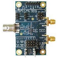
SDI Input and SDO Output
The SDI input connector (J1) is a 75Ω BNC connector. The SDI input should conform to the SMPTE 424M,
SMPTE 292M, or SMPTE 259M standards.
The SDO output connectors (J2 and J3) are 50Ω SMA connectors. When using only one side of the output pair,
the other side should be terminated with a 50Ω SMA termination. For example, when only using the SDO output,
¯¯¯¯ should be terminated with a 50Ω SMA termination.
SDO
DC Power Connectors
The VCC and GND power connectors should be powered with a DC input voltage of 3.3V ± 5% (3.6V maximum).
SPI Mode / Pin Mode Select (JP1 – JP4)
JP1, JP2, JP3, and JP4 are used to select between SPI Mode or Pin mode. To select Pin Mode, set four jumpers
as shown in Figure 2, and to select SPI Mode, set four jumpers as shown in Figure 3. Either Pin Mode or SPI
mode must be selected for proper operation; do not leave JP1-JP4 open.
Figure 2. Pin Mode Select
Figure 3. SPI Mode Select
MUTE
(JP5)
REF
JP5 allows control of the MUTE
function and may be used in either Pin Mode or SPI Mode. MUTE
is an input
REF
REF
¯¯¯ . The MUTE
voltage used to set the threshold for CD
DC input voltage should be between 0V and 3.3V. Refer
REF
to the LMH0384 datasheet for details. Leave JP5 unconnected for normal operation.
Pin Mode Controls (JP6 – JP8)
JP6, JP7, and JP8 are used to control LMH0384 features while the device is configured for Pin Mode. Jumpers
should not be placed on JP6, JP7, or JP8 while the device is configured for SPI Mode.
¯¯¯ and MUTE (JP6)
CD
¯¯¯ ) monitoring and MUTE control. CD
¯¯¯ is high when no input signal is present. MUTE
JP6 allows Carrier Detect (CD
¯¯¯ to allow automatic mute operation based on the input
may be used to force the outputs on or off, or tied to CD
signal. To activate mute and force the outputs into a muted condition, set the jumper to pull MUTE to VCC. To turn
off mute so that the outputs will never mute, set the jumper to tie MUTE to GND. For normal operation, set the
¯¯¯ to MUTE for automatic mute control. The LMH0384 MUTE pin has an internal pulldown (to
jumper to tie CD
disable mute), so JP6 may be left unconnected and the LMH0384 will never mute.
SD384 EVK User Guide
2 of 5
Rev 1.2
© 2009, National Semiconductor Corp.
Related parts for SD384EVK
Image
Part Number
Description
Manufacturer
Datasheet
Request
R

Part Number:
Description:
National Semiconductor [8-Bit D/A Converter]
Manufacturer:
National Semiconductor
Datasheet:
Part Number:
Description:
National Semiconductor [Media Coprocessor]
Manufacturer:
National Semiconductor
Datasheet:
Part Number:
Description:
Digitally Controlled Tone and Volume Circuit with Stereo Audio Power Amplifier, Microphone Preamp Stage and National 3D Sound
Manufacturer:
National Semiconductor
Datasheet:
Part Number:
Description:
Digitally Controlled Tone and Volume Circuit with Stereo Audio Power Amplifier, Microphone Preamp Stage and National 3D Sound
Manufacturer:
National Semiconductor
Datasheet:
Part Number:
Description:
AC97 Rev 2 Codec with Sample Rate Conversion and National 3D Sound
Manufacturer:
National Semiconductor
Part Number:
Description:
Manufacturer:
National Semiconductor
Datasheet:
Part Number:
Description:
Manufacturer:
National Semiconductor
Datasheet:
Part Number:
Description:
General Purpose, Low Voltage, Low Power, Rail-to-Rail Output Operational Amplifiers
Manufacturer:
National Semiconductor
Datasheet:
Part Number:
Description:
8-bit 20 MSPS flash A/D converter.
Manufacturer:
National Semiconductor
Datasheet:
Part Number:
Description:
Low Noise Quad Operational Amplifier
Manufacturer:
National Semiconductor
Datasheet:
Part Number:
Description:
Quad Differential Line Receivers
Manufacturer:
National Semiconductor
Datasheet:
Part Number:
Description:
Quad High Speed Trapezoidal? Bus Transceiver
Manufacturer:
National Semiconductor
Datasheet:
Part Number:
Description:
Dual Line Receiver
Manufacturer:
National Semiconductor
Datasheet:
Part Number:
Description:
TTL to 10k ECL Level Translator with Latch
Manufacturer:
National Semiconductor
Datasheet: