CP2120EK Silicon Laboratories Inc, CP2120EK Datasheet - Page 17
CP2120EK
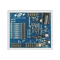
Manufacturer Part Number
CP2120EK
Description
KIT EVAL FOR CP2120
Manufacturer
Silicon Laboratories Inc
Specifications of CP2120EK
Main Purpose
Interface, SPI to I²C
Utilized Ic / Part
CP2120
Processor To Be Evaluated
CP2120
Interface Type
SPI
Lead Free Status / RoHS Status
Contains lead / RoHS non-compliant
Secondary Attributes
-
Embedded
-
Primary Attributes
-
Lead Free Status / Rohs Status
Lead free / RoHS Compliant
Other names
336-1325


6.4. I
Bytes received from I
inside this buffer is saved in the RXBUFF Internal Register.
6.5. I
SPI commands initiate all I
command has been successfully received across the SPI bus. Once the CP2120 has completed the I
transaction prompted by the command, the INT pin will be pulled low to indicate that command execution has
completed. If an I
ignored.
6.5.1. Write Bytes to I
This command transmits data to an I
followed by the number of bytes to be transmitted across I
the I
was indicated by the second byte of the command will result in an error condition, and the I2C transaction will not
be initiated.
Once the I
the results of the transaction.
6.5.2. Read Bytes from I
This command attempts to retrieve bytes from an I
0x01, followed by the number of bytes to read (1 to 255) and the address of the I
Once the I
the transaction. The CP2120 saves the number of bytes stored in the buffer in the internal register named
RXBUFF. A Read Buffer command can be issued to retrieve the bytes from the buffer.
Note that if the SPI Master issues a second Read Bytes from I
command, the bytes stored in the CP2120's buffer will be overwritten.
Internal Register Address: 0x06
2
C Slave. The SPI master then sends the data to be transmitted across I
2
2
C Receive Buffer Size
C Commands
RXB7
2
2
Bit 7
C transaction completes, the CP2120 pulls the INT pin low and sets I2CSTAT according to the results of
C transaction completes, the CP2120 pulls the INT pin low and sets the internal register according to
SPI Master
R
Internal Register Definition 6. RXBUFF: Receive Buffer Size Register
Reset Value:
2
C command is issued while an I
Bit 7-0:
2
C transactions are stored in the 255-byte data buffer. The number of bytes currently stored
RXB6
2
C
Bit 6
R
2
COMMAND
C
SPI Master
2
C transactions. The CP2120 executes I
0x00
RXB7-0: Receive Buffer Size
Indicates the number of bytes received during the last I
0x00
RXB5
Bit 5
R
2
OF BYTES
NUMBER
C slave device. The command begins with the command byte (0x00),
COMMAND
0x01
RXB4
Bit 4
R
2
C Slave device. The command begins with the command byte,
2
C command is in progress, the second I
ADDRESS +W
Rev. 0.4
SLAVE
OF BYTES
NUMBER
2
C, which can range from 1 to 255, and the address of
RXB3
Bit3
R
2
C command before issuing a Read Buffer
2
SLAVE ADDRESS
C transactions only after every byte of the
BYTE1
DATA
RXB2
Bit 2
R
2
+R
C. Sending more or fewer bytes than
2
C slave device.
...
RXB1
2
Bit 1
C read transaction.
R
BYTE N
2
DATA
C command will be
CP2120
RXB0
Bit 0
R
2
17
C
Related parts for CP2120EK
Image
Part Number
Description
Manufacturer
Datasheet
Request
R

Part Number:
Description:
QFN 20/I°/SPI-I2C BRIDGE AND GPIO PORT EXPANDER
Manufacturer:
Silicon Laboratories Inc

Part Number:
Description:
IC I/O EXPANDER I2C/SPI 8B 20QFN
Manufacturer:
Silicon Laboratories Inc
Datasheet:
Part Number:
Description:
SMD/C°/SINGLE-ENDED OUTPUT SILICON OSCILLATOR
Manufacturer:
Silicon Laboratories Inc
Part Number:
Description:
Manufacturer:
Silicon Laboratories Inc
Datasheet:
Part Number:
Description:
N/A N/A/SI4010 AES KEYFOB DEMO WITH LCD RX
Manufacturer:
Silicon Laboratories Inc
Datasheet:
Part Number:
Description:
N/A N/A/SI4010 SIMPLIFIED KEY FOB DEMO WITH LED RX
Manufacturer:
Silicon Laboratories Inc
Datasheet:
Part Number:
Description:
N/A/-40 TO 85 OC/EZLINK MODULE; F930/4432 HIGH BAND (REV E/B1)
Manufacturer:
Silicon Laboratories Inc
Part Number:
Description:
EZLink Module; F930/4432 Low Band (rev e/B1)
Manufacturer:
Silicon Laboratories Inc
Part Number:
Description:
I°/4460 10 DBM RADIO TEST CARD 434 MHZ
Manufacturer:
Silicon Laboratories Inc
Part Number:
Description:
I°/4461 14 DBM RADIO TEST CARD 868 MHZ
Manufacturer:
Silicon Laboratories Inc
Part Number:
Description:
I°/4463 20 DBM RFSWITCH RADIO TEST CARD 460 MHZ
Manufacturer:
Silicon Laboratories Inc
Part Number:
Description:
I°/4463 20 DBM RADIO TEST CARD 868 MHZ
Manufacturer:
Silicon Laboratories Inc
Part Number:
Description:
I°/4463 27 DBM RADIO TEST CARD 868 MHZ
Manufacturer:
Silicon Laboratories Inc
Part Number:
Description:
I°/4463 SKYWORKS 30 DBM RADIO TEST CARD 915 MHZ
Manufacturer:
Silicon Laboratories Inc