CY3272 Cypress Semiconductor Corp, CY3272 Datasheet - Page 17
CY3272
Manufacturer Part Number
CY3272
Description
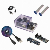
KIT EVAL POWERLINE HIGH VOLT
Manufacturer
Cypress Semiconductor Corp
Datasheet
1.CY3272.pdf
(34 pages)
Specifications of CY3272
Main Purpose
Interface, Transceiver, Powerline Communication
Embedded
No
Utilized Ic / Part
CY8CPLC10
Primary Attributes
2400bps Data Transfer Over High Voltage Power Lines
Secondary Attributes
LED Status Indicators
Silicon Manufacturer
Cypress
Silicon Core Number
CY8CPLC10
Kit Application Type
Communication & Networking
Application Sub Type
High Voltage Powerline Communication
Rohs Compliant
Yes
Lead Free Status / RoHS Status
Lead free / RoHS Compliant
Lead Free Status / RoHS Status
Lead free / RoHS Compliant, Lead free / RoHS Compliant
Other names
428-3008


2.4.2
2.4.3
CY3272 Cypress High Voltage Powerline Communication Evaluation Kit Guide, Doc. # 001-55381 Rev. *C
Manual addressing is an easy method to quickly assign a particular address between 0 and 7 to the
board which may be a node in a network.
Note After changing the address of the node, the RESET button on the board must be pressed on
the PLC HV Board for the change to take effect.
Setting Up I2C Address of the Node
I2C DIP switch S1[2] is used to assign a specific I2C address to the node for communicating with the
external microcontroller/PSoC or USB-I2C bridge. When the I2C switch S1[2] is in the OFF position,
the address of the node is 0x01 and when it is in the ON position, the address of the node is 0x7A.
For further details on I2C addressing, refer to the device data sheet, which is on the CD.
I2C Header Settings
The I2C header, J5, is a five pin header that can be used for communicating with an external board,
powering an external board, and resetting the CY8CPLC10 device from an external board. A five
wire ribbon cable is provided with this kit for use on the J5 header. The description for J5 header pins
is as follows:
Table 2-5. J5 I2C Header Pins
Figure 2-7. I2C Header for Communication
V – Vdd
G – Gnd
D – I2C Data (SDA)
C – I2C Clock (SCL)
R – Reset
J5 Pin Name
The Vdd pin can provide a maximum of 50 mA at 5 V to an external board. It is only
to source the current. DO NOT SUPPLY POWER TO THIS PIN FOR POWERING
THE CY8CPLC10 DEVICE. Note that the PWR jumper, as explained in the next
section, needs to be connected to enable this functionality.
The Gnd pin can provide the ground reference to an external board. This pin con-
nects to the ground of the CY3272 board.
The I2C Data (SDA) pin is the data line for the I2C communication. This pin is
directly connected to the I2C_SDA pin on the CY8CPLC10 device. Check the next
section for appropriate jumper settings for I2C communication through this pin.
The I2C Clock (SCL) pin is the clock line for the I2C communication. This pin is
directly connected to the I2C_SCL pin on the CY8CPLC10 device. Check the next
section for appropriate jumper settings for I2C communication through this pin.
Connecting the reset of an external board to this pin enables the resetting of the
CY8CPLC10 device via the external board. Note that RES jumper, as explained in
the next section, needs to be connected to enable this functionality.
Description
PLC HV Evaluation Board
17
[+] Feedback
Related parts for CY3272
Image
Part Number
Description
Manufacturer
Datasheet
Request
R

Part Number:
Description:
Manufacturer:
Cypress Semiconductor Corp
Datasheet:
Part Number:
Description:
Manufacturer:
Cypress Semiconductor Corp
Datasheet:
Part Number:
Description:
Manufacturer:
Cypress Semiconductor Corp
Datasheet:
Part Number:
Description:
Manufacturer:
Cypress Semiconductor Corp
Datasheet:
Part Number:
Description:
Manufacturer:
Cypress Semiconductor Corp
Datasheet: